NPN & PNP Transistors explained - electronics engineering
Summary
TLDRThis educational video script delves into the fundamentals of bipolar transistors, highlighting the two primary types: NPN and PNP. It explains the structure of these devices, which consist of three pins (emitter, base, and collector) and are often encased in resin for protection. The script clarifies the difference between the two types by detailing the arrangement of n-type and p-type materials, which form the critical pn junction. It further illustrates the functioning of each transistor type with examples, demonstrating how current flows and is controlled within circuits. The video also provides guidance on how to identify the emitter pin and how to interpret transistor symbols in electrical diagrams, encouraging viewers to continue their exploration of electronics engineering through additional resources and social media platforms.
Takeaways
- 🔍 There are two main types of bipolar transistors: NPN and PNP, which look similar but can be differentiated by checking the part number.
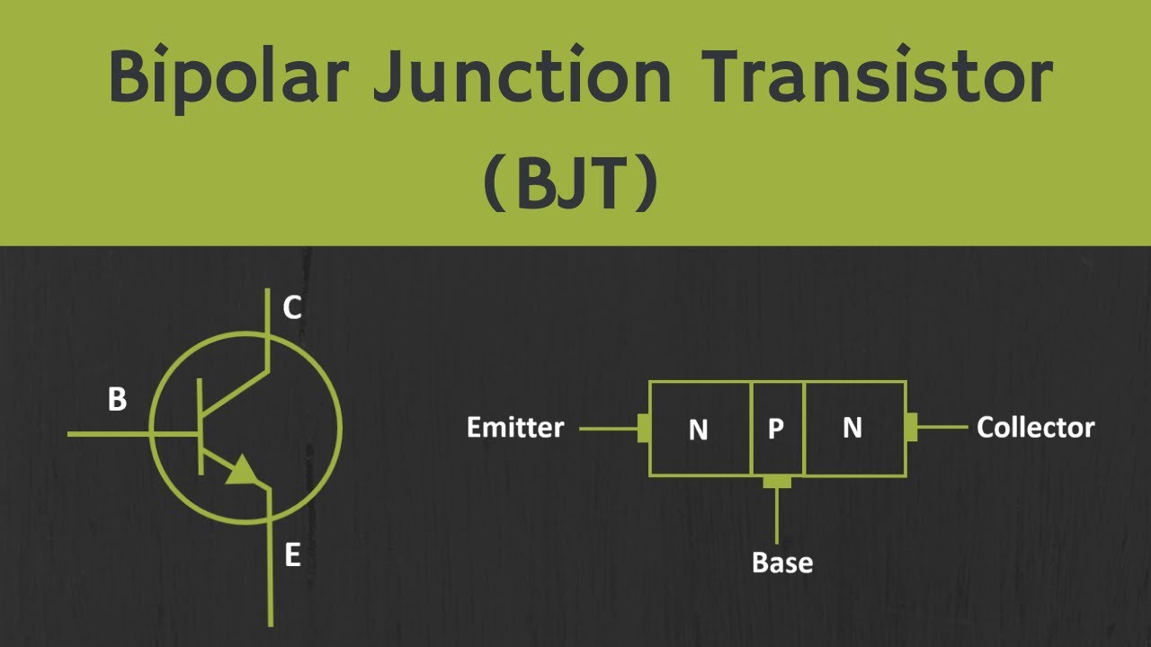
- 📍 Transistors have three pins labeled E (emitter), B (base), and C (collector), and their arrangement can vary, so it's important to consult the manufacturer's data sheet.
- 💊 Silicon is doped with other materials to create P-type and N-type materials, which are combined to form the PN junction, essential for transistor operation.
- 🛡️ The transistor's structure consists of layers of P-type and N-type materials, with NPN having two N-type layers and one P-type layer, and PNP being the reverse.
- 🏗️ The transistor is encased in resin to protect its internal components.
- 🔋 In an NPN transistor, the main and control circuits are connected to the positive side of the battery, and the transistor turns on when the control circuit switch is pressed.
- 🔌 With a PNP transistor, the emitter is connected to the positive side of the battery, and the transistor's operation involves current flowing out of the base and through the main circuit.
- 🔄 In the given example, the NPN transistor combines current (5mA base, 20mA collector, 25mA emitter), while the PNP transistor divides current (25mA emitter, 20mA collector, 5mA base).
- 📊 Transistors are represented on electrical diagrams with symbols that include an arrow pointing in the direction of conventional current flow.
- 👨🏫 The video encourages viewers to continue learning about electronics engineering by following suggested channels and websites.
Q & A
What are the two main types of bipolar transistors?
-The two main types of bipolar transistors are the NPN and the PNP type.
How can you differentiate between an NPN and a PNP transistor physically?
-Physically, NPN and PNP transistors look nearly identical, so you need to check the part number to tell which is which.
What do the labels E, B, and C on a transistor represent?
-The labels E, B, and C on a transistor represent the emitter, the base, and the collector, respectively.
What is the typical pin configuration for a transistor with a flat edge?
-For a transistor with a flat edge, the left pin is typically the emitter, the middle is the base, and the right side is the collector.
Why is it important to check the manufacturer's data sheet for transistors?
-It is important to check the manufacturer's data sheet for transistors because not all transistors use the standard pin configuration, and the data sheet provides specific information about the transistor's configuration and usage.
What is doping in the context of semiconductor material?
-Doping in the context of semiconductor material refers to the process of adding a small amount of another material to pure silicon to change its electrical properties, creating p-type and n-type materials.
What is the purpose of the pn junction in a transistor?
-The pn junction in a transistor is formed by combining p-type and n-type materials. It is the fundamental structure that allows the transistor to control the flow of current.
How is the internal configuration of an NPN transistor different from a PNP transistor?
-In an NPN transistor, there are two layers of n-type material with one layer of p-type material (the base) in between. In a PNP transistor, the configuration is the opposite, with two layers of p-type material surrounding one layer of n-type material.
What happens when the switch is pressed in the control circuit of an NPN transistor?
-When the switch is pressed in the control circuit of an NPN transistor, the main circuit turns on, allowing current to flow from the battery through the transistor and the main LED, and then back to the battery.
How does the current flow differ in a PNP transistor compared to an NPN transistor?
-In a PNP transistor, when the switch is pressed, some of the current flows out of the base pin and returns to the battery, while the rest of the current flows through the transistor and the main LED, then back to the battery. This is different from an NPN transistor, where the current combines within the transistor.
What is the significance of the arrow in the electrical symbol for a transistor?
-The arrow in the electrical symbol for a transistor is placed on the emitter and points in the direction of conventional current. This helps to indicate how to connect the transistor into circuits correctly.
How can one continue learning about electronics engineering after watching the video?
-To continue learning about electronics engineering after watching the video, one can click on one of the videos on screen, follow the provided social media channels, and visit engineeringmindset.com for more lessons.
Outlines

Esta sección está disponible solo para usuarios con suscripción. Por favor, mejora tu plan para acceder a esta parte.
Mejorar ahoraMindmap

Esta sección está disponible solo para usuarios con suscripción. Por favor, mejora tu plan para acceder a esta parte.
Mejorar ahoraKeywords

Esta sección está disponible solo para usuarios con suscripción. Por favor, mejora tu plan para acceder a esta parte.
Mejorar ahoraHighlights

Esta sección está disponible solo para usuarios con suscripción. Por favor, mejora tu plan para acceder a esta parte.
Mejorar ahoraTranscripts

Esta sección está disponible solo para usuarios con suscripción. Por favor, mejora tu plan para acceder a esta parte.
Mejorar ahoraVer Más Videos Relacionados

Transistors - Field Effect and Bipolar Transistors: MOSFETS and BJTs

Transistors Explained - How transistors work

What is a Transistor | Working Principles
Introduction to Bipolar Junction Transistor (BJT)

Bipolar Junction Transistor

Transistor Introduction (Bipolar Transistors & its Biasing) Basic Electronics
5.0 / 5 (0 votes)
