Transistors Explained - How transistors work
Summary
TLDRThis video script delves into the intricate workings of transistors, a pivotal invention in electronics. It distinguishes between bipolar and field effect transistors, focusing on the bipolar type, and explains their dual role as switches and amplifiers. The script covers the physical aspects of transistors, including casing and heat dissipation, and details the function of the emitter, base, and collector. It illustrates how a small voltage at the base can control a larger current, highlighting the transistor's amplifying capability. The explanation extends to the difference between NPN and PNP transistors, their symbolic representation, and a foundational understanding of semiconductors and PN junctions, concluding with the transistor's operation analogous to a water pipe with a controllable gate.
Takeaways
- 🌟 Transistors are pivotal electronic components that can act as switches and amplifiers.
- 🔍 There are two main types of transistors: bipolar and field-effect, with a focus on bipolar in this video.
- 🛡️ Transistors come in various forms, with low power ones in plastic cases and high power ones in metal cases for heat dissipation.
- 🔍 The metal body transistors are often attached to heat sinks to prevent damage from heat generated during operation.
- 📝 Each transistor has a part number which is crucial for referencing the manufacturer's datasheet for specifications.
- 🔌 Transistors have three pins labeled E (emitter), B (base), and C (collector), with the configuration varying by model.
- 🔄 Transistors control current flow; a small voltage at the base can turn the transistor on or off, acting as an electronic switch.
- 📡 The base pin requires a minimum voltage, typically 0.6V to 0.7V, to initiate the flow of current in the main circuit.
- 🔗 Transistors can amplify signals; a small change in base voltage results in a significant change in the main circuit, functioning as an amplifier.
- 🔢 The current gain, symbolized by beta, is the ratio of collector current to base current and can be found in the datasheet.
- 🔁 There are NPN and PNP types of bipolar transistors, which differ in their current flow direction and require checking the part number to distinguish.
- 💡 Transistors are represented with symbols in electrical diagrams, with the arrow indicating the direction of conventional current flow.
- 🌐 Understanding how a transistor works involves the concept of electron flow, which is opposite to the conventional current direction.
- 🚀 The operation of a transistor is analogous to controlling water flow with a gate, where the gate's opening is analogous to the base voltage affecting the main circuit's current.
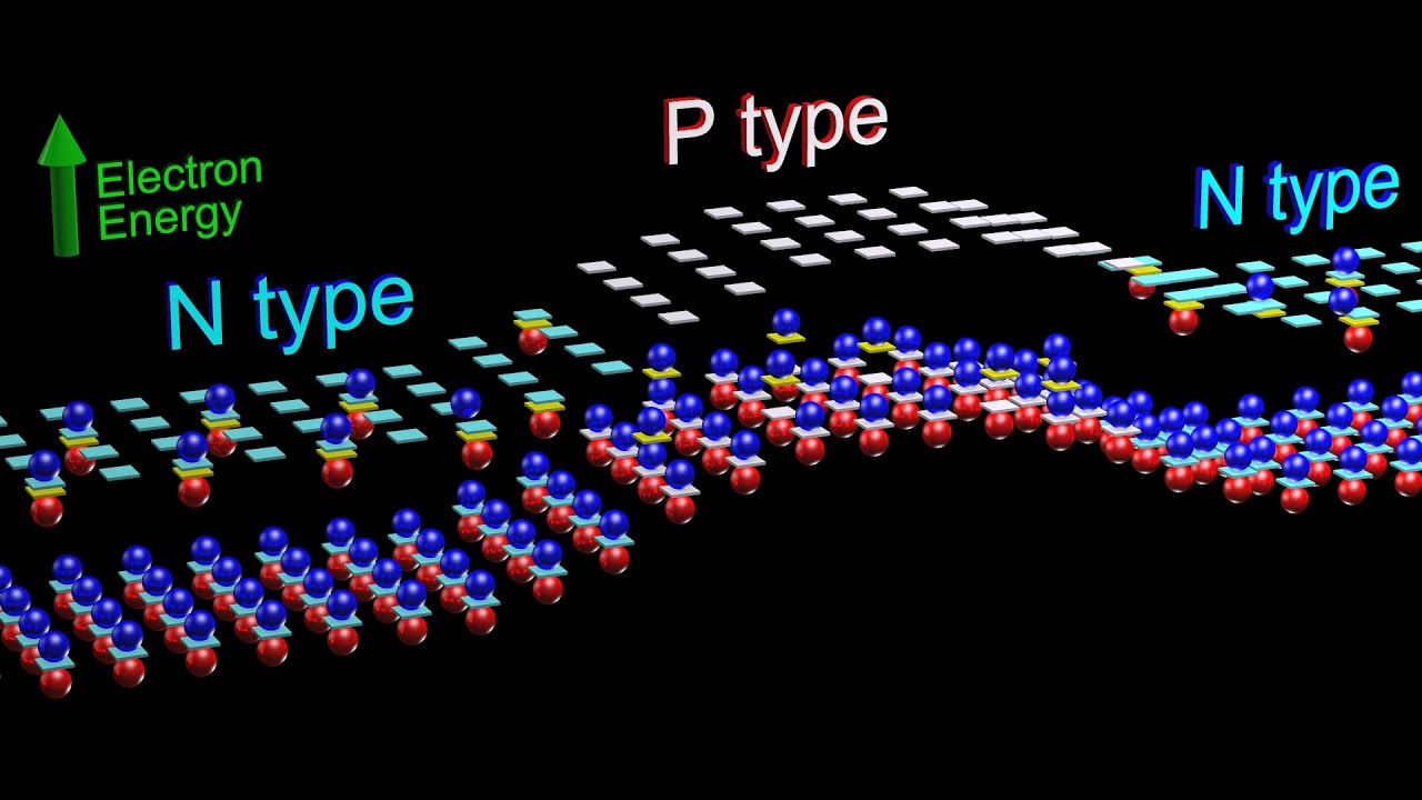
- 🌗 The PN junction forms the core of a transistor, with N-type and P-type materials creating a barrier that can be influenced by external voltage.
- 💼 Engineers use doping to alter silicon's properties, creating N-type and P-type semiconductors that are essential for transistor function.
Q & A
What is the significance of the transistor in the field of electronics?
-The transistor is one of the most important devices ever invented, playing a crucial role in modern electronics due to its ability to act as a switch and amplify signals, which are fundamental functions in controlling and processing electrical currents in circuits.
What are the two main types of transistors mentioned in the script?
-The two main types of transistors mentioned are bipolar and field-effect transistors, with the script primarily focusing on the bipolar version.
What are the two primary functions of a transistor?
-A transistor can act as a switch to control circuits and also amplify signals, making it a versatile component in electronic devices.
Why are higher power transistors often enclosed in a metal case?
-Higher power transistors are enclosed in a metal case to help dissipate the heat generated during operation, which is crucial to prevent damage to the internal components over time.
What is the purpose of attaching metal body transistors to a heat sink?
-Heat sinks are used to enhance the heat dissipation from metal body transistors, ensuring that the components do not overheat and maintain their performance and longevity.
What information can be found on the body of a transistor?
-The body of a transistor typically has text indicating the part number, which can be used to reference the manufacturer's datasheet for detailed specifications and ratings of the transistor.
What are the three pins of a transistor labeled as, and what do they represent?
-The three pins of a transistor are labeled as E for emitter, B for base, and C for collector, representing the different points of electrical connection within the transistor.
Why is it important to check the manufacturer's datasheet for a transistor?
-The manufacturer's datasheet provides essential information about the transistor's voltage and current ratings, ensuring that it is used safely and within its operational limits.
What is the minimum voltage typically required to turn on a transistor?
-Typically, at least 0.6V to 0.7 volts is required to be applied to the base pin for the transistor to turn on and start conducting current in the main circuit.
How does a transistor act as an amplifier?
-A transistor acts as an amplifier by using a small voltage and current at the base pin to control a larger voltage and current in the main circuit, thus amplifying the input signal.
What is the current gain of a transistor, and how can it be determined?
-The current gain of a transistor, symbolized by beta, is the ratio of the collector current to the base current. It can be found in the manufacturer's datasheet or calculated using the formula beta = collector current / base current.
What is the difference between NPN and PNP transistors in terms of current flow?
-In an NPN transistor, the current combines as it flows from the emitter through the base to the collector. In contrast, in a PNP transistor, the current divides, flowing out of the emitter, through the base, and out of the collector.
How are the symbols for transistors represented in electrical drawings?
-Transistors are represented with symbols that include an arrow pointing in the direction of conventional current flow, indicating how they should be connected in circuits.
What is the analogy used in the script to explain the working principle of an NPN transistor?
-The script uses the analogy of water flowing through a pipe with a swing gate in a smaller pipe to explain how an NPN transistor works, where the gate represents the base controlling the flow in the main pipe, analogous to the base controlling the current flow in the transistor.
What is the role of doping in semiconductor materials like silicon?
-Doping is the process of adding impurities to pure silicon to change its electrical properties. P-type doping introduces materials with fewer valence electrons, creating 'holes', while N-type doping introduces materials with extra valence electrons, creating free electrons, which influences the semiconductor's conductivity.
How does the PN junction form in a semiconductor, and what is the depletion region?
-The PN junction forms when P-type and N-type semiconductor materials are joined together. At the junction, a depletion region is created where excess electrons from the N-side move to occupy holes on the P-side, forming a barrier with a built-up charge on either side, which creates an electric field preventing further movement of charge carriers.
What happens when a forward bias is applied to a PN junction?
-When a forward bias is applied to a PN junction, the voltage source causes the barrier to collapse, allowing electrons to flow from the N-type side to the P-type side, enabling current to flow through the junction.
What is the purpose of the emitter in an NPN transistor during operation?
-In an NPN transistor, the emitter's role is to provide a large number of excess electrons due to heavy doping, which, when a forward bias is applied, rushes across to fill the space within the P-type material, initiating the transistor's conduction process.
Outlines

This section is available to paid users only. Please upgrade to access this part.
Upgrade NowMindmap

This section is available to paid users only. Please upgrade to access this part.
Upgrade NowKeywords

This section is available to paid users only. Please upgrade to access this part.
Upgrade NowHighlights

This section is available to paid users only. Please upgrade to access this part.
Upgrade NowTranscripts

This section is available to paid users only. Please upgrade to access this part.
Upgrade NowBrowse More Related Video

¿Cómo funciona el TRANSISTOR?

Transistors, How do they work?

Basic electronics Guide to components in Hindi

What is Electronics | Introduction to Electronics | Electronic Devices & Circuits

Transistor Introduction (Bipolar Transistors & its Biasing) Basic Electronics

Semiconductors - Physics inside Transistors and Diodes
5.0 / 5 (0 votes)