SEM Optimization, Astigmatism Correction, and Basic Electron Optics
Summary
TLDRIn this video, the presenter provides a detailed overview and demonstration of scanning electron microscopy (SEM) at extremely high magnifications, reaching the nanometer scale. Covering basic electron optics, SEM operation principles, and machine components like the electron column, electron gun, and objective aperture, the video explains key parameters such as acceleration voltage, probe current, working distance, and sample tilt. It also addresses common imaging challenges, including astigmatism and aberrations, and demonstrates step-by-step optimization techniques to achieve high-resolution images of gold nanoparticles. The tutorial concludes with practical tips for fine-tuning SEM settings to capture precise, clear images.
Takeaways
- 😀 The process of obtaining high-resolution images from an SEM involves understanding complex electron optics and non-ideal factors in the microscope.
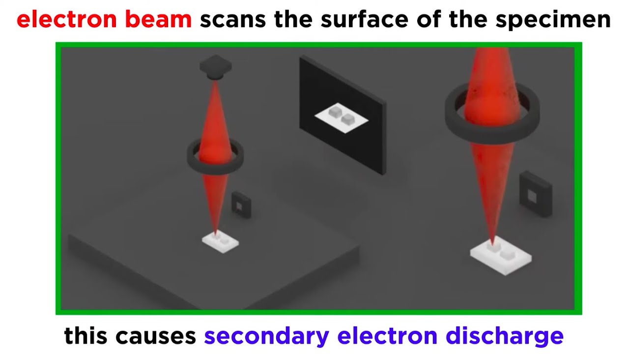
- 😀 The electron microscope operates with an electron gun that generates and accelerates electrons down a column, striking the sample and generating signals for imaging.
- 😀 The microscope's column includes electron optics (coils) that focus and deflect the electron beam, but they can introduce aberrations like astigmatism and chromatic imperfections.
- 😀 Two types of electron microscopes: thermionic emission (Tungsten filament) and field emission, with field emission offering higher resolution but harder maintenance.
- 😀 SEM resolution can be influenced by factors like acceleration voltage, probe current, working distance, sample tilt, and objective aperture size.
- 😀 Higher acceleration voltage (30 kV) reduces aberrations but can obscure surface detail as electrons penetrate deeper into the sample.
- 😀 Decreasing the probe current reduces spot size and sample damage, leading to sharper images with lower beam energy loss.
- 😀 Working distance affects resolution: lowering it brings the sample closer to the electron beam, reducing aberrations and increasing contrast.
- 😀 Tilting the sample at 30-45 degrees increases secondary electron count and contrast, especially useful when reducing spot size and image clarity.
- 😀 Adjusting the objective aperture allows control over probe current and spot size, crucial for achieving optimal image quality at different magnifications.
Q & A
What is the basic principle behind how an SEM produces images?
-An SEM produces images by accelerating electrons from an electron gun down the microscope column to strike a sample. Secondary electrons emitted from the sample are detected and synchronized with the scanning system to generate the image.
What is the role of electron optics in an SEM?
-Electron optics, composed of coils that generate electric and magnetic fields, focus, accelerate, and deflect the electron beam. They shape the beam similar to how glass lenses shape light, but imperfections can cause aberrations.
What are the main types of electron emission sources in SEMs, and how do they differ?
-The main types are thermionic emission (tungsten filament) and field emission. Field emission offers higher brightness, lower energy spread, and better resolution, but is more complex to maintain. Thermionic emission is easier to use but provides lower resolution.
How does acceleration voltage affect SEM imaging?
-Higher acceleration voltage decreases aberrations and probe size, improving resolution, but penetrates deeper into the sample, potentially reducing surface detail. Lower voltage emphasizes surface features but reduces overall resolution.
What is probe current and spot size, and why are they important?
-Probe current is the total current of electrons hitting the sample, and spot size is the diameter of the electron beam. Lower probe current reduces spot size, increases resolution, and minimizes sample damage, while higher probe current increases signal but can blur details.
What is astigmatism in an SEM, and how is it corrected?
-Astigmatism occurs when electrons passing through different parts of the lens are not focused in the same plane, causing a blurry spot. It is corrected using stigmators, which generate weak perpendicular fields to stretch or skew the beam, achieving a circular, focused spot.
Why is sample tilt used, and how does it affect image quality?
-Tilting the sample (typically 30–45°) increases secondary electron emission and reduces edge effects, improving contrast and brightness, especially when using small spot sizes for high-resolution imaging.
What is the objective aperture, and what effect does changing its size have?
-The objective aperture is a metal plate with micron-scale holes that restricts the electron beam. Smaller apertures reduce probe current and spot size, increasing resolution and reducing aberrations, but can decrease signal intensity.
What is the recommended workflow to optimize SEM imaging for high resolution?
-The workflow includes saturating the filament, setting a short working distance, tilting the sample, selecting and centering the smallest objective aperture, setting a high acceleration voltage, aligning the gun, focusing, adjusting stigmators for astigmatism, selecting small spot size/probe current, and performing a slow scan.
How are gold nanoparticles used in SEM optimization?
-Gold nanoparticles, 5–20 nm in size, are used as a standard to check resolution, contrast, and astigmatism correction. Proper imaging of these particles indicates optimal alignment and settings of the SEM.
What are spatial and chromatic aberrations in an SEM, and how do they impact image quality?
-Spatial aberrations occur when magnetic fields are non-uniform, causing electrons to focus imperfectly. Chromatic aberrations arise from variations in electron energy. Both distort the image and limit resolution, but can be minimized by adjusting acceleration voltage and probe settings.
Why is it important to perform slow scanning for high-resolution SEM images?
-Slow scanning allows the electron beam to collect more data per pixel line, reducing noise and improving the clarity and detail of high-resolution images, whereas fast scanning provides a quick preview but lower resolution.
Outlines

This section is available to paid users only. Please upgrade to access this part.
Upgrade NowMindmap

This section is available to paid users only. Please upgrade to access this part.
Upgrade NowKeywords

This section is available to paid users only. Please upgrade to access this part.
Upgrade NowHighlights

This section is available to paid users only. Please upgrade to access this part.
Upgrade NowTranscripts

This section is available to paid users only. Please upgrade to access this part.
Upgrade NowBrowse More Related Video

Introduction to the Scanning Electron Microscope (SEM)

Temp1 Cap1 Epi3 Microscopía Electrónica

Scanning Electron Microscopy (SEM) | Working Principles and application of SEM in biology
Electron Microscopy (TEM and SEM)

Introduction to Scanning Electron Microscopy (SEM)
Pengujian Alat SEM - Scanning Electron Microscope
5.0 / 5 (0 votes)