Introduction to the Scanning Electron Microscope (SEM)
Summary
TLDRThis video provides an overview of Scanning Electron Microscopy (SEM) and Environmental Scanning Electron Microscopy (ESEM). It explains how SEM uses electrons instead of visible light to generate highly detailed images of samples, focusing on secondary and backscattered electrons. The script compares coated and uncoated samples, discusses issues like charging, and demonstrates the advantages of ESEM for imaging wet samples. Practical steps for sample preparation, imaging in different modes, and the differences between secondary electron and backscatter imaging are illustrated through a salt crystal experiment.
Takeaways
- ๐ฌ SEM and ECM use electrons instead of visible light for imaging, providing higher resolution due to the shorter wavelength of electrons.
- ๐ก In a light microscope, glass lenses focus and detect light, whereas SEM uses an electron gun and electromagnetic lenses.
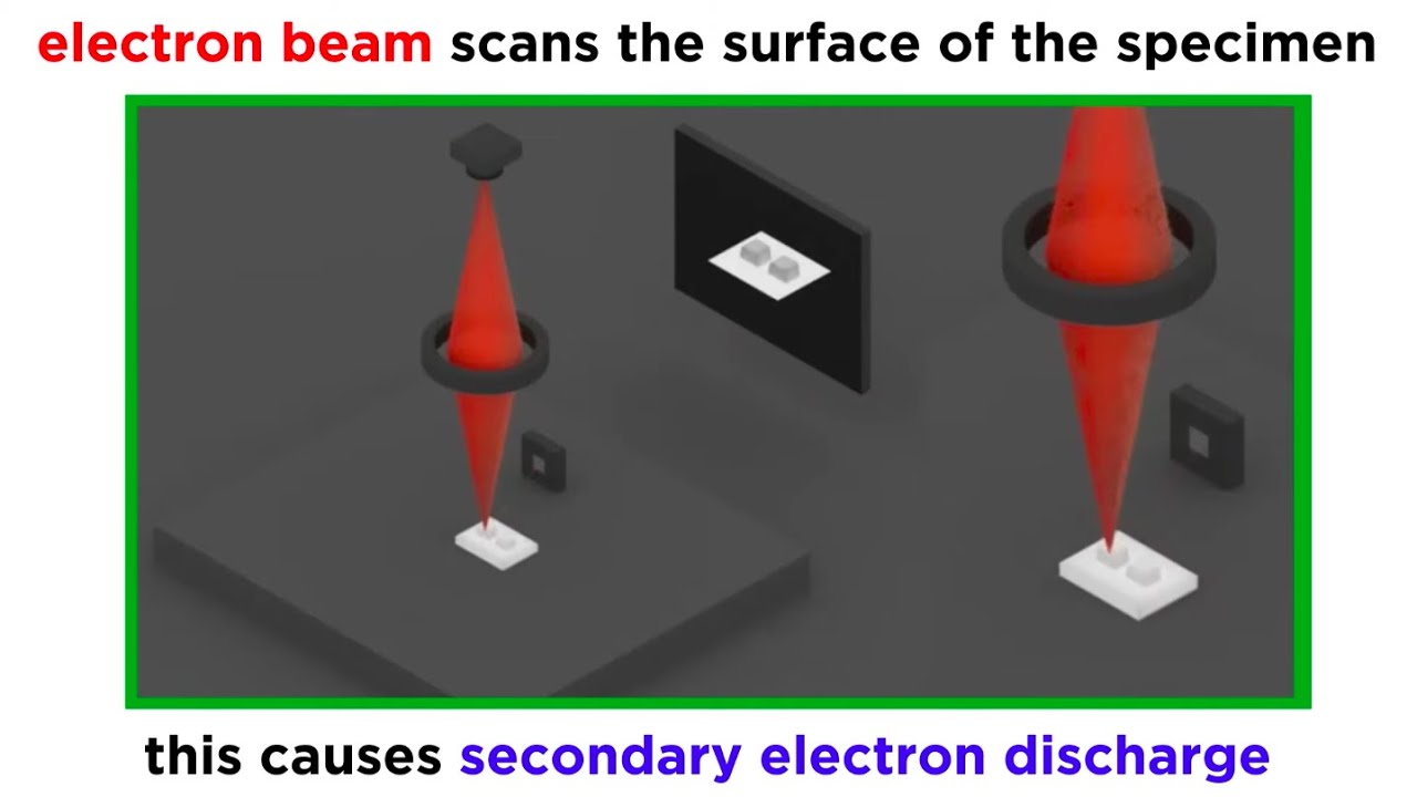
- ๐ธ SEM images are usually formed by detecting secondary electrons, which show surface features and produce a 3D-like effect.
- โก Charging occurs in samples when the number of electrons hitting and leaving the sample is unequal, which can be prevented by coating with a thin layer of metal.
- ๐ SEM can image features as small as 1-2 nanometers and as large as 1-2 millimeters, with scale bars indicating sizes in images.
- ๐ฏ Backscatter electron images highlight differences in atomic number, with regions of higher atomic number appearing brighter.
- ๐ง Traditional SEM requires a vacuum and dry samples, while ECM allows for imaging of wet samples by introducing water vapor.
- ๐ฟ ECM is particularly useful for imaging biological samples like cells and bacteria without distorting them by drying.
- โ๏ธ Conductive samples do not require coating in SEM, while non-conductive samples are often coated to prevent charging issues.
- ๐ SEM can operate in various modes, including high vacuum, low vacuum, and environmental SEM, offering flexibility for different sample types.
Q & A
What is the main difference between SEM and ECM?
-The main difference between SEM (Scanning Electron Microscopy) and ECM (Environmental Scanning Electron Microscopy) is that SEM operates in a high vacuum, while ECM allows the introduction of water vapor into the vacuum chamber, making it suitable for imaging wet samples without drying them.
Why do electron microscopes use electrons instead of visible light?
-Electron microscopes use electrons instead of visible light because electrons have a much shorter wavelength, allowing for higher resolution imaging that can visualize smaller features compared to traditional optical microscopes.
What is charging in the context of SEM, and why is it a problem?
-Charging occurs when the number of electrons that strike the sample is not equal to the number of electrons that leave the sample. This causes a buildup of electrical charge, which negatively affects the quality of the image, often making it blurry or distorted.
How is charging prevented in SEM?
-Charging is often prevented by coating non-conductive samples with a thin layer of metal, such as gold-palladium, to allow electrons to flow away from the sample, preventing charge buildup.
What are the two main types of electrons detected in SEM, and what information do they provide?
-The two main types of electrons detected in SEM are secondary electrons and backscattered electrons. Secondary electrons provide information about the surface topology, offering 3D-like images, while backscattered electrons provide information on atomic number contrasts, often appearing flatter and showing brighter areas for materials with higher atomic numbers.
What advantages does ECM have over traditional SEM?
-ECM allows for imaging wet or biological samples without needing to dry them out, preserving their natural state. It also helps prevent charging on non-conductive samples by introducing water vapor into the chamber.
Why is a vacuum necessary in SEM imaging?
-A vacuum is necessary in SEM imaging because electrons used for imaging would scatter off gas molecules in the air, preventing the electron beam from being focused on the sample and resulting in poor image quality.
What is the purpose of the sputter coater in SEM sample preparation?
-The sputter coater deposits a thin layer of conductive material, such as gold-palladium, onto non-conductive samples to prevent charging during SEM imaging, ensuring high-quality images.
What kind of samples benefit from being imaged in ECM mode?
-Biological and wet samples, such as cells, bacteria, and plant tissues, benefit from being imaged in ECM mode, as they can remain hydrated and be imaged in their natural state without drying or coating.
What difference is seen between secondary electron and backscattered electron images?
-Secondary electron images highlight the surface features of a sample, creating a more 3D appearance. Backscattered electron images emphasize atomic number contrasts, with regions of higher atomic numbers appearing brighter, and the images generally looking flatter.
Outlines
๐ฌ Introduction to SEM and ECM
Carrie Dumbly, the director of Chapel Hill Analytical and Nanofabrication Lab, introduces scanning electron microscopy (SEM) and environmental scanning electron microscopy (ECM). Unlike optical microscopes, which use visible light, SEM and ECM use electrons to create images, offering higher resolution due to the shorter wavelength of electrons. She explains how SEM and ECM use electron beams to interact with samples, producing backscattered and secondary electrons, which are key in generating detailed images. She also mentions the issue of sample charging and how coating samples with a thin metal layer prevents image distortion.
๐ Imaging Wet Samples with ECM
This section focuses on the challenges and advantages of imaging wet samples using ECM. Traditional SEM requires samples to be dry due to the need for a vacuum, which distorts wet samples. However, ECM allows for a controlled amount of water vapor in the chamber, enabling the imaging of hydrated biological samples like cells and bacteria. Though ECM resolution is lower than that of traditional SEM due to electron scattering by water molecules, it allows for imaging without drying out the samples or requiring conductive coatings.
๐งช Sample Preparation for SEM Imaging
Catherine McInnis, a graduate student, demonstrates how to prepare a sample for SEM imaging. The process involves mounting the sample on a stub with conductive tape, usually carbon or copper tape. Non-conductive samples require a conductive coating, typically applied using a sputter coater that deposits a thin metal layer (gold-palladium) on the sample. McInnis walks through the sputter coating process and explains how a quartz crystal microbalance helps measure the amount of deposited material, ensuring that a sufficient coating is applied to prevent charging during SEM imaging.
๐ธ Imaging Salt Crystals Using SEM and ECM
This section covers the imaging of salt crystals using SEM in high vacuum, low vacuum, and environmental modes. The high vacuum mode produces clear images of coated salt crystals, while uncoated salt shows signs of charging, making imaging difficult. In low vacuum mode, introducing water vapor prevents charging, enabling clear imaging of uncoated salt. In ECM mode, the humidity level is adjusted to form water droplets, demonstrating how salt dissolves and recrystallizes. The section also compares images captured with secondary and backscatter electron detectors, highlighting differences in surface topology and atomic number contrasts.
๐ง๏ธ SEM and ECM Imaging Modes
This final section wraps up the demonstration of SEM and ECM imaging modes. The uncoated salt sample showed charging issues in high vacuum mode, but switching to low vacuum mode eliminated this effect. In ECM mode, increasing humidity dissolved the salt crystals, and reducing it caused recrystallization. The section also compares secondary electron and backscatter electron images of the same sample, showing the difference in surface detail and atomic number contrasts, with secondary electrons emphasizing surface features and backscatter electrons highlighting atomic number differences.
Mindmap
Keywords
๐กScanning Electron Microscopy (SEM)
๐กEnvironmental Scanning Electron Microscopy (ECM)
๐กElectrons
๐กBackscattered Electrons
๐กSecondary Electrons
๐กCharging
๐กVacuum
๐กConductive Coating
๐กSputter Coating
๐กAtomic Number Contrast
Highlights
Introduction to Scanning Electron Microscopy (SEM) and Environmental Scanning Electron Microscopy (ECM), focusing on using electrons instead of visible light for imaging.
Electrons have a much shorter wavelength than visible light, allowing SEM and ECM to achieve higher resolutions than traditional optical microscopes.
SEM uses backscattered and secondary electrons to produce images, highlighting how different electron interactions provide various imaging results.
Charging occurs when the number of electrons striking a sample differs from the number leaving it, potentially distorting the image. Coating non-conductive samples with a thin layer of metal can prevent charging.
Secondary electron images reveal surface features in great detail, showing three-dimensional structures, as seen in the zinc oxide nanowire image.
Backscattered electron images focus more on differences in atomic number, making regions with higher atomic numbers appear brighter, such as barium titanate particles in a polymer sample.
SEM is capable of imaging features as small as 1-2 nanometers and as large as 1-2 millimeters, making it versatile for various applications.
A comparison between secondary and backscatter SEM images of a polymer resin circuit board with soldered connections shows how each technique highlights different aspects of the same sample.
Environmental SEM allows imaging of wet samples like biological cells and bacteria without needing to dry them out, preserving their natural state.
Using an ECM with controlled water vapor can prevent charging for non-conductive samples without needing a conductive coating, which is advantageous for imaging.
Demonstration of how environmental SEM can dissolve and recrystallize salt crystals by adjusting the humidity in the chamber, showing the systemโs versatility.
Switching between secondary electron detectors and backscatter electron detectors provides contrasting views of the same sample, enhancing analysis.
Uncoated samples can show streaks and artifacts due to charging, demonstrating the importance of proper sample preparation for SEM imaging.
Sputter coating with gold palladium is used to make non-conductive samples conductive, preventing charging during SEM imaging.
A discussion on optimizing SEM imaging conditions, including focusing the electron beam and adjusting stigmation, ensures high-quality images.
Transcripts
[Music]
welcome my name is Carrie dumbly and I'm
the director of the Chapel Hill
analytical and nanofabrication lab or
channel at UNC today we will be talking
about scanning electron microscopy often
called SEM an environmental scanning
electron microscopy often called ECM the
SEM and ECM are microscopes that produce
images using electrons instead of
visible light
remember the wavelength of light limits
the resolution in an optical microscope
today we're going to learn about using
electrons which have a much shorter
wavelength than visible light for
imaging purposes this is a diagram of a
light microscope the basic components
include a light source a way to focus
that light onto the sample a way to
collect the light that travels through
the sample and a way to detect that
light with a light microscope glass
lenses similar to magnifying glasses are
used to focus the light and collect the
light an electron microscope has many of
the same components as a light
microscope instead of a light source the
electron microscope uses an electron gun
to produce electrons electromagnetic
lenses are used to focus the electrons
and the detector is sensitive to
electrons instead of visible light
electrons can interact with a sample in
a number of ways today we will focus on
the backscattered and secondary
electrons that we can detect in an
electron microscope when an electron
beam strikes a sample some of the
electrons are absorbed other electrons
are back scattered and some sample
electrons can be ejected as secondary
electrons if the number of electrons
that strike the sample is not equal to
the number of electrons that leave the
sample then the sample will build up a
charge this is called charging and it
negatively affects the quality of the
resulting image in order to prevent
charging many SEM samples are coated
with a thin layer of metal
most SEM images are produced by
collecting secondary electrons this
image is a secondary electron image of
zinc oxide nanowires and nano flowers
secondary electron images show the
surface features of a sample and
therefore look very three-dimensional
the scale bar at the bottom right of the
image indicates that most of these
nanowires are a few microns long and
only 50 to 100 nanometers wide this is
another secondary electron image showing
cells that were cultured on top of
manufactured pillars notice that the
scale bar for this image is much larger
than the previous image scanning
electron microscopes can typically image
features as small as one or two
nanometers and as large as one or two
millimeters backscatter SCM images show
fewer surface features than secondary
electron images often back scatter
images look very flat the contrast that
we do see in a back scattered image is
due to differences in average atomic
number regions of the sample with higher
atomic number will produce more
backscattered electrons and appear
bright this image is of a polymer sample
sample with barium titanate particles
embedded in it since the barium titanate
has a much higher average atomic number
these particles appear much brighter
than the polymer that they are embedded
in many electron microscopes have both
secondary and backscatter electron
detectors and acquiring both images on
the same sample can illustrate the
differences between them this sample is
a polymer resin circuit board with some
soldered connections the secondary
electron image on the Left shows the
surface topology while the backscattered
image on the right shows the atomic
number contrasts it is clear that the
bright regions are from the higher
atomic number solder which is composed
primarily of tin both types of images
provide useful information
in a typical SEM vacuum is required
because the electrons that we use for
imaging will scatter off gas molecules
and prevent us from focusing the
electron beam on the sample as a result
we can only image dry samples in a
typical SEM if we want to look at wet
samples we need to dry them out first
and this often distorts their shape this
image shows how there are very few
residual gas molecules in the SEM
chamber of a traditional SEM and the
beam spot on the samples is relatively
small an environmental SEM often called
an ECM allows the operator to introduce
a controllable amount of water vapor
into the SEM vacuum chamber there is one
disadvantage of using an environmental
SEM when you introduce water molecules
into the chamber the electrons that are
traveling towards the sample will hit
these water molecules and scatter the
result is that the electron beam is not
as tightly focused as in a traditional
low-pressure SEM thus the resolution of
the images is not as good the main
advantage of an ECM is that you can
image wet samples without having to dry
them out these include many types of
biological samples such as cells
bacteria and plants in the ECM we can
keep these samples hydrated and image
them in their natural state in addition
we can use a small amount of water vapor
to also prevent charging this allows us
to image non conductive samples without
the need for a conductive coating this
is an ECM image of a bacterial biofilm
the bacteria are the rod shaped
particles that are about one micron long
the ECM is great for imaging these types
of wet samples thank you for joining
this discussion of scanning electron
microscopy and environmental scanning
electron microscopy
you
[Music]
welcome I'm Carrie Donnelly the director
of the Chapel Hill analytical and nano
fabrication lab or channel at UNC with
me today is Catherine McInnis a graduate
student at UNC hello everyone thanks for
joining us today I'm going to show you
how to prepare samples for scanning
electron microscopy or SEM let's head to
the law welcome to the SEM lab today we
will be imaging some salt crystals the
tools that we will need to prepare our
sample for imaging today include the
sample tweezers sample stubs conductive
tape two common types are carbon tape
and copper tape and possibly a sputter
coder first I'll mount the sample onto a
sample stub with some conductive tape
the tape I'm using is double-sided
carbon tape and I'll use it to hold the
salt in place
by gently tapping the sample stub on the
table I can remove any excess salt that
is not well attached samples that are
not conductive need to be coated with a
conductive coating for traditional SEM
imaging in order to prevent charging
problems our lab uses a sputter coder to
deposit a thin layer of gold palladium
but some labs use a carbon coating
instead I'll place the sample in the
sputter coder the metal that we will
deposit is actually held in the lid in
this small circular disk just next to
the sample is called a quartz crystal
microbalance it can measure how much
material has been deposited after
loading the sample into the chamber and
closing the lid I can evacuate the
chamber using a vacuum pump once the
chamber has been evacuated I can start
the deposition a plasma is generated
that removes material from the gold
palladium target and deposits it
everywhere in the chamber including on
my sample it's easier to see this plasma
if we turn off the lights the readout
from the quartz crystal microbalance
lets me know how much material has been
deposited a 2 nanometer coating is
usually sufficient to prevent charging
if your sample is conductive or if you
will be imaging in an environmental SEM
you can skip the sample coating step our
sample is now ready for SEM imaging
let's head to the imaging lab
[Music]
hello I'm Kerry Donnelly the director of
the Chapel Hill analytical and nano
fabrication lab or channel at UNC with
me today is Catherine McInnis a graduate
student at UNC in this section we will
show you how to image a sample with
scanning electron microscopy or SEM and
environmental scanning electron
microscopy or ECM I prepared our salt
sample for imaging and now I'm ready to
look at it with the SEM
welcome to the SEM lab this is the SEM
that we will be using today it can
operate in three different modes high
vacuum low vacuum and environmental SEM
mode we will image in all three modes
today remember the SEM operates under
vacuum so first I will bent the chamber
to atmosphere and then load the sample
the sample stub has a small post that
fits into the sample stage a small set
screw holds the sample in place I'm also
going to load a similar salt sample that
hasn't been coated with any metal so we
can compare the effect of the metal
coating on imaging most systems take
just a minute or two before they are
pumped down to a low enough pressure to
start imaging
I'll start by imaging in high vacuum
mode this is the standard operating mode
for most SEMS the first thing to do when
starting to image is to focus the
electron beam on the sample
I will also adjust the stig nation to
make sure that I'm imaging with a round
beam of electrons and not an ellipse and
make sure my imaging conditions are
optimized once these things are done it
is pretty easy to move around on the
sample and zoom in or zoom out the scale
bar at the bottom right of the image
lets me know how big the features in my
sample are these particles are on the
order of 100
of microns this sample is traditional
table salt and you can see from this
image I collected that it crystallizes
into nice square crystals common table
salt is sodium chloride and its crystal
structure is face centered cubic as
shown here it's easy to see how the
arrangement of atoms and sodium chloride
results in the small cubes that we see
by SEM imaging now let's move to the
uncoated salt crystals this image of the
uncoated salt shows some streaks and
some bright and dark spots that don't
quite look right this is the charging
effect that we discussed earlier because
the sample is not conductive it is
building up a charge and this makes it
very difficult to image it properly with
a charged beam of electrons it would be
impossible to collect a good image under
these conditions
now we're going to switch to low vacuum
mode and continue to image the uncoated
salt sample remember that in low vacuum
mode we introduce some water vapor in
the chamber that will help prevent
charging this is the same area of the
sample we were just looking at and you
can see that now I can collect a much
nicer image than I could in high vacuum
mode let's now operate the system in
environmental SEM mode for this we'll
need to use a different sample stage
that is capable of cooling the sample
and a slightly different sample holder
in which I can put some uncoated salt
crystals once the system has pumped down
to the pressure that will image at we
can start to adjust the humidity level
in the chamber you can see that at some
point the chamber becomes humid enough
to start forming water droplets on the
salt crystals if I let the water
continue to form on the sample the salt
crystal will eventually dissolve into
the water I can force the salt to
recrystallize by reducing the humidity
in the chamber and allowing the water to
evaporate once it does the salt will
form crystals again all of the imaging
I've done so far has all been with a
secondary electron detector if I switch
to the backscatter detector it's clear
that the conch
mechanism is different these two images
are of the same salt crystals but with
two different detectors the one on the
left is a typical secondary electron
image showing the surface topology the
image on the right is a backscatter
image which shows more atomic number
contrasts the salt crystals become
relatively dark because sodium and
chlorine have lower atomic numbers than
the metal sample holder that they are
sitting in this image is also much
flatter looking than the secondary
electron image thank you for joining us
for this demonstration of sem and ECM
imaging today we image coated and
uncoated salt samples in high vacuum
mode and saw charging on the uncoated
sample we successfully used low vacuum
mode to eliminate charging in isa mode
we increase the humidity enough to form
water droplets that could dissolve the
salt and then decrease the humidity in
the chamber and saw the salt
recrystallize finally we saw the
difference between images obtained with
a secondary electron detector and a
backscatter electron detector
Browse More Related Video
Electron Microscopy (TEM and SEM)
Introduction to Scanning Electron Microscopy (SEM)
Instrumen Analisis - 6
How do Electron Microscopes Work? ๐ฌ๐ ๐ฌ Taking Pictures of Atoms
Particulate Formation, Evolution, and Fate -Michelson Day 2 Part 3
1.1 - Introduction to transmission electron microscopy (TEM)
5.0 / 5 (0 votes)