U1_L2_P-N Junction Diode | Electronics Engineering (BEC101/201)| Hindi
Summary
TLDRThe transcript appears to be a lecture on semiconductor basics, focusing on the concept of the depletion layer in PN junction diodes. It discusses the formation of depletion layers when P-type and N-type semiconductors are combined, leading to the creation of an electric field barrier. The lecture explores the impact of forward and reverse biasing on the depletion layer, explaining how it affects the flow of current. Key terms like forward bias, reverse bias, and breakdown voltage are introduced, providing foundational knowledge for understanding diode behavior in electronic circuits.
Takeaways
- 😀 The lecture discusses the basics of semiconductors, specifically focusing on the PN junction diode.
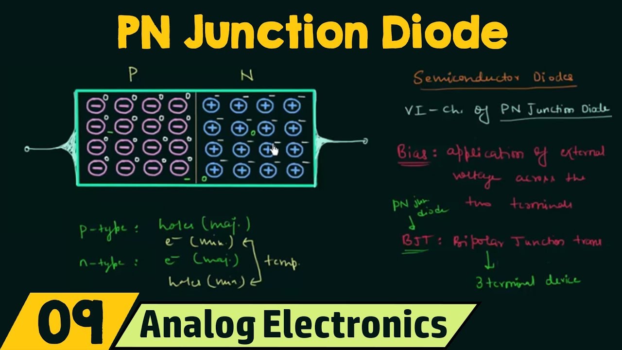
- 🔬 The difference between N-type and P-type semiconductors is explained, with N-type having majority charge carriers of electrons and P-type having majority charge carriers of holes.
- 🌐 The concept of diffusion and drift currents is introduced, explaining how these currents contribute to the functioning of a diode.
- 💡 The formation of a depletion layer at the PN junction is described, which acts as a barrier for the movement of charge carriers.
- 🔋 The effect of applying a battery source to a PN junction diode is explored, detailing the processes of forward and reverse biasing.
- 📈 The behavior of the depletion layer under different biases is explained, showing how it can either increase or decrease depending on the applied voltage.
- 🛠️ The concept of forward and reverse breakdown voltages is introduced, which are critical values that determine the diode's operation.
- 🔌 The practical implications of understanding the PN junction diode are highlighted, including its importance in various electronic devices.
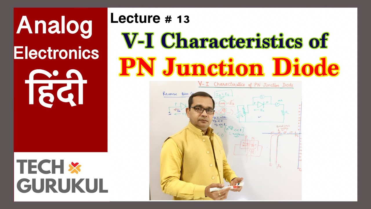
- 📊 The lecture also touches on the symbolic representation of diodes in circuit diagrams and how to analyze current-voltage characteristics.
- 🔬 The theoretical framework behind the formation of the PN junction and the concept of displacement layer is discussed.
Q & A
What is the basic concept of a semiconductor?
-A semiconductor is a material that has electrical conductivity between that of a conductor and an insulator. The conductivity of semiconductors can be precisely controlled by the addition of impurities in the form of dopants, which makes them essential for electronic devices.
What are the two main types of charge carriers in semiconductors?
-The two main types of charge carriers in semiconductors are electrons and holes. Electrons are negatively charged, while holes are positive charge carriers that result from the absence of an electron in a semiconductor's crystal lattice.
What is the significance of the depletion layer in a p-n junction?
-The depletion layer in a p-n junction is significant because it forms a region devoid of free charge carriers, creating a potential barrier that prevents further movement of charge carriers. This layer plays a crucial role in the functioning of diodes and transistors.
What is the forward biasing of a p-n junction, and how does it affect the depletion layer?
-Forward biasing a p-n junction involves applying a voltage across the junction such that the p-type side is connected to the positive terminal and the n-type side to the negative terminal of a battery. This causes the depletion layer to thin, allowing more charge carriers to cross the junction and increasing the current flow.
What happens to the depletion layer when a reverse bias is applied to a p-n junction?
-When a reverse bias is applied to a p-n junction, the depletion layer widens. This is because the applied voltage opposes the natural flow of charge carriers, causing the barrier between the p and n regions to increase and reducing the current flow.
What is the term used to describe the minimum voltage required to turn on a diode?
-The term used to describe the minimum voltage required to turn on a diode is the 'forward voltage' or 'threshold voltage.' For silicon diodes, this is typically around 0.7 volts, while for germanium diodes, it is around 0.3 volts.
How does the reverse breakdown voltage relate to the operation of a diode?
-The reverse breakdown voltage is the maximum reverse voltage that a diode can withstand before it breaks down and allows a significant reverse current to flow. This voltage is critical for the safe operation of diodes in circuits to prevent damage from excessive reverse voltages.
What is the role of the intrinsic semiconductor in the formation of a p-n junction?
-The intrinsic semiconductor plays a role in the formation of a p-n junction by providing the pure semiconductor material that is then doped to create the p-type and n-type regions. The intrinsic semiconductor is characterized by having equal concentrations of electrons and holes.
What is the difference between a p-type and an n-type semiconductor?
-A p-type semiconductor is doped with an element that has fewer valence electrons than silicon, creating an excess of holes, while an n-type semiconductor is doped with an element that has more valence electrons than silicon, creating an excess of electrons.
How does the doping process influence the electrical properties of a semiconductor?
-Doping a semiconductor introduces impurities that either donate extra electrons (n-type doping) or create holes where electrons can move into (p-type doping), thereby significantly altering the material's electrical conductivity and enabling the creation of p-n junctions and other semiconductor devices.
Outlines

Cette section est réservée aux utilisateurs payants. Améliorez votre compte pour accéder à cette section.
Améliorer maintenantMindmap

Cette section est réservée aux utilisateurs payants. Améliorez votre compte pour accéder à cette section.
Améliorer maintenantKeywords

Cette section est réservée aux utilisateurs payants. Améliorez votre compte pour accéder à cette section.
Améliorer maintenantHighlights

Cette section est réservée aux utilisateurs payants. Améliorez votre compte pour accéder à cette section.
Améliorer maintenantTranscripts

Cette section est réservée aux utilisateurs payants. Améliorez votre compte pour accéder à cette section.
Améliorer maintenantVoir Plus de Vidéos Connexes

PN Junction Diode (No Applied Bias)

Varactor (Construction & Working) Special Purpose Diode (Basic Electronics) BE/BTech 1st year

V-I Characteristics of PN Junction Diode in Hindi | TECH GURUKUL By Dinesh Arya

Schottky Diode (Construction & Working) Special Purpose Diodes (Basics Electronics)

Lab 4 and 5: PN junctions and Solar Cells

Semiconductor PN Junctions, The Depletion Region and Diode Characteristics
5.0 / 5 (0 votes)
