Schottky Diode (Construction & Working) Special Purpose Diodes (Basics Electronics)
Summary
TLDRThis video explains the operation and characteristics of PN junction diodes and Schottky diodes. It covers the behavior of current flow, the creation of the depletion region, and the concept of potential barriers in diodes. The script delves into forward and reverse biasing, highlighting the importance of overcoming the potential barrier for current to flow. Additionally, it compares Schottky diodes to PN junction diodes, emphasizing their advantages in high-frequency applications due to their faster switching and unipolar current flow. Overall, the video provides a detailed yet accessible explanation of semiconductor behavior in diode circuits.
Takeaways
- 😀 The script discusses a specialized topic about semiconductor devices, focusing on PN junction diodes and their properties.
- 😀 The concept of a depletion layer and its effect on the electric field and potential barrier in a PN junction diode is explained.
- 😀 It is highlighted that the forward voltage drop for a PN junction diode is typically around 0.7V, which is necessary to allow current to flow.
- 😀 The importance of the potential barrier (0.7V) and how it prevents current flow until a sufficient battery voltage is applied is explained.
- 😀 A distinction is made between bipolar and unipolar devices, with emphasis on how current flows differently in each type.
- 😀 The script introduces the concept of a high-frequency switching diode and its advantages, including faster switching times.
- 😀 The script also talks about the significance of metal-semiconductor junctions and their application in creating a better quality diode.
- 😀 The forward and reverse biasing of diodes is explained in terms of how they affect the electric field and current flow.
- 😀 The importance of material selection, such as using metals like aluminum or platinum in semiconductor devices, is mentioned.
- 😀 The breakdown voltage and potential drop across the junction are crucial factors for understanding the behavior of the diode under different conditions.
Q & A
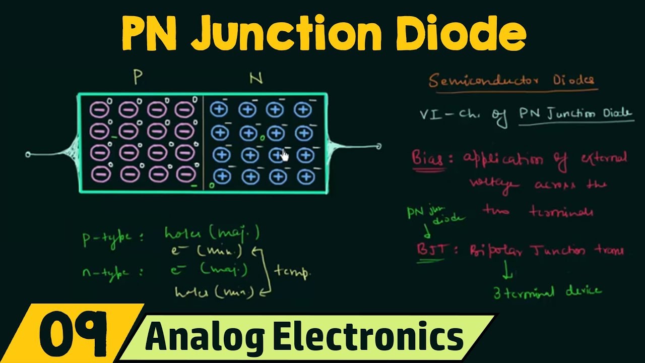
What is a PN junction diode?
-A PN junction diode is formed when a P-type semiconductor and an N-type semiconductor are connected together. The junction between them is known as the PN junction.
What happens when a P-type and N-type semiconductor are connected?
-When a P-type and N-type semiconductor are connected, the electrons and holes diffuse across the junction, creating a depletion region where charge carriers are absent.
What is the depletion region in a PN junction?
-The depletion region in a PN junction is the area around the junction where charge carriers (electrons and holes) have diffused away, leading to a shortage of charge and forming an electric field.
Why is the potential barrier important in a PN junction diode?
-The potential barrier is important because it prevents current from flowing easily through the diode under certain conditions. It typically requires a minimum voltage (about 0.6 to 0.7V) to overcome this barrier and allow current to flow.
What is the significance of the forward voltage drop in a PN junction diode?
-The forward voltage drop refers to the voltage required to overcome the potential barrier of the diode. In a PN junction, this drop is typically around 0.7V, which allows current to flow when the diode is forward-biased.
How does the forward bias affect the current flow in a PN junction diode?
-In forward bias, when the positive terminal of a battery is connected to the P-type material and the negative terminal to the N-type material, the potential barrier is reduced, allowing current to flow through the diode.
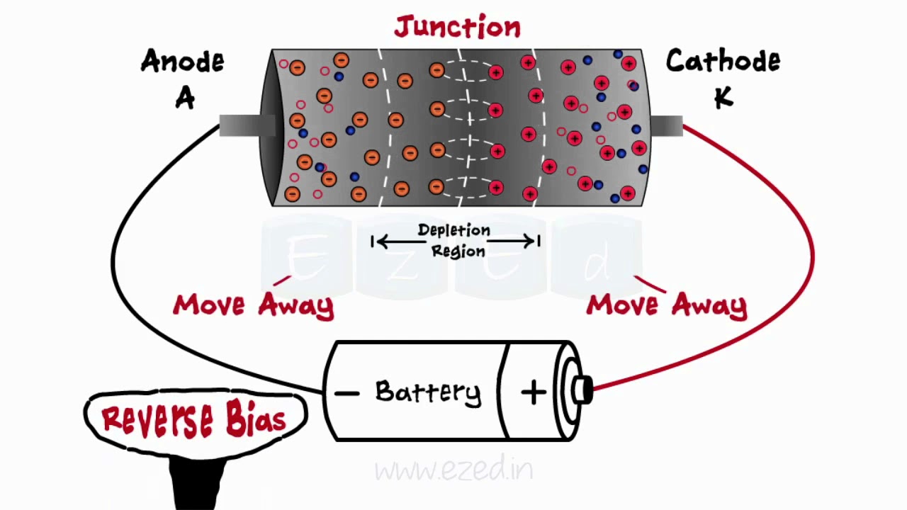
What happens when the PN junction diode is reverse biased?
-In reverse bias, the P-type material is connected to the negative terminal of the battery and the N-type to the positive terminal. This increases the potential barrier, preventing current flow, except for a small leakage current.
What is the difference between a bipolar and a unipolar device?
-A bipolar device involves both electrons and holes as charge carriers, such as in a PN junction diode. A unipolar device, on the other hand, uses only one type of charge carrier (either electrons or holes), like in a Metal-Oxide-Semiconductor Field-Effect Transistor (MOSFET).
What role does the electric field play in a PN junction diode?
-The electric field in the depletion region of a PN junction diode is crucial in preventing the free movement of charge carriers, thus creating the potential barrier that must be overcome for current to flow.
Why is the breakdown voltage significant in a PN junction diode?
-The breakdown voltage is the voltage at which the PN junction diode will break down and allow significant current to flow in reverse bias, often leading to damage if the voltage exceeds the diode's rated capacity.
Outlines

This section is available to paid users only. Please upgrade to access this part.
Upgrade NowMindmap

This section is available to paid users only. Please upgrade to access this part.
Upgrade NowKeywords

This section is available to paid users only. Please upgrade to access this part.
Upgrade NowHighlights

This section is available to paid users only. Please upgrade to access this part.
Upgrade NowTranscripts

This section is available to paid users only. Please upgrade to access this part.
Upgrade NowBrowse More Related Video
Types of Diodes - The Learning Circuit
PN Junction Diode (No Applied Bias)
Diodes - What Are Diodes - PN Junction - Forward Bias - Reverse Bias - Zener Diodes

Lab 4 and 5: PN junctions and Solar Cells

Semiconductor PN Junctions, The Depletion Region and Diode Characteristics

Forward Bias (P N Junction Diode) Diode theory & applications (Basic Electronics)
5.0 / 5 (0 votes)