Semiconductor PN Junctions, The Depletion Region and Diode Characteristics
Summary
TLDRThis video introduces the concept of semiconductors, focusing on silicon and its atomic structure. It explains the role of doping in creating p-type and n-type materials, which form the PN Junction, the core component of diodes. The video covers the importance of the depletion region and the effects of forward and reverse bias on conductivity. The behavior of diodes in these conditions is illustrated, showing how current flow is enabled when the depletion region collapses at a certain voltage. Future videos will explore Zener diodes, bipolar junction transistors, and field-effect transistors.
Takeaways
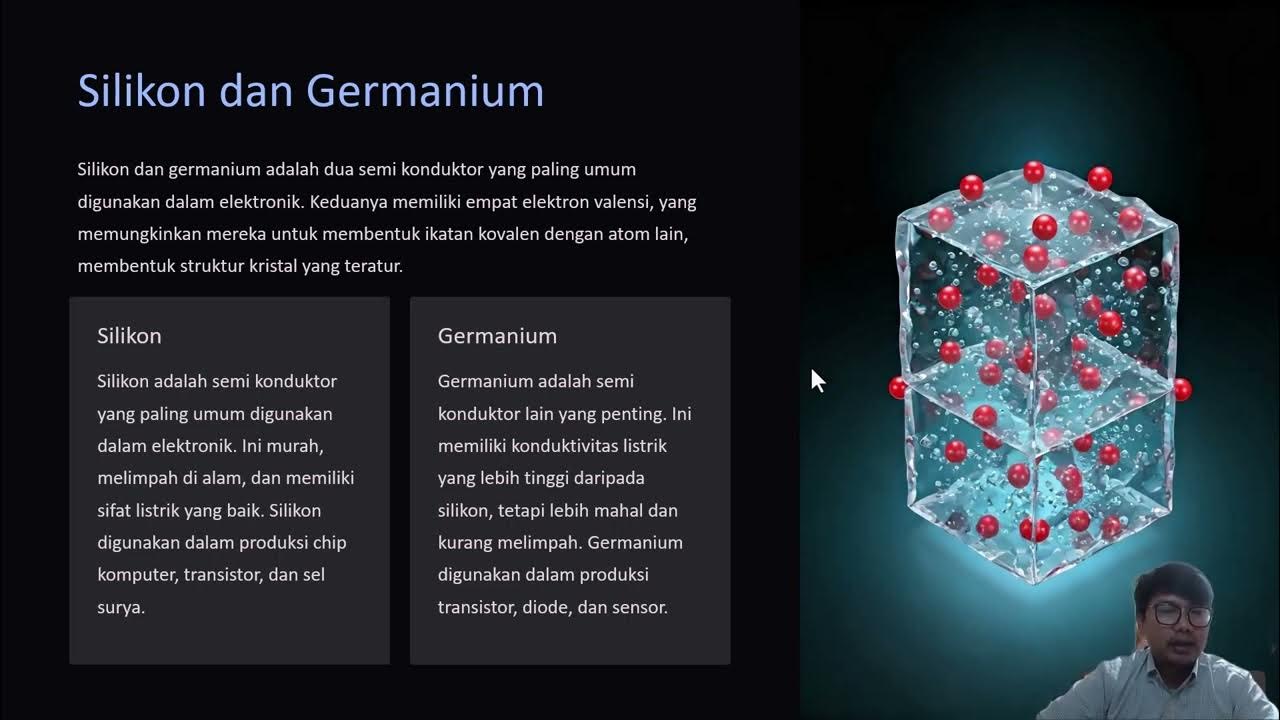
- 😀 Silicon is a key material in semiconductors, with a crystalline structure held together by four covalent bonds.
- 😀 Electron fusion in silicon involves the continuous breaking and forming of bonds, with higher temperatures increasing the rate of this process.
- 😀 Doping adds impurities to silicon, creating p-type (positive) and n-type (negative) materials based on the number of bonds required by the atoms.
- 😀 P-type material has a deficit of electrons (holes), while n-type material has excess free electrons.
- 😀 The PN Junction is formed when p-type and n-type materials are joined, with the p-type being rich in holes and the n-type having free electrons.
- 😀 The depletion region at the junction is where no free electrons exist, resulting in high resistance and preventing current flow.
- 😀 Diffusion causes electrons to move and form new bonds, while drift opposes this movement and encourages electrons to stay in place.
- 😀 Forward bias in a PN Junction reduces the depletion region and allows current to flow, while reverse bias increases the depletion region and prevents current flow.
- 😀 Diodes require a certain activation voltage (around 0.6V to 0.7V) to collapse the depletion region and allow current to pass through in forward bias.
- 😀 The relationship between current and voltage in a diode is nonlinear, with current increasing rapidly once the activation voltage is reached.
- 😀 The video will later cover additional semiconductor devices like Zener diodes, bipolar junction transistors, and field-effect transistors (FETs).
Q & A
What is the main focus of the video?
-The video introduces the concept of semiconductors, focusing on the PN Junction and its relationship to simple semiconductor devices such as diodes, with mentions of Zener diodes, bipolar Junction transistors, and field effect transistors in future videos.
Why are semiconductors important in modern electronics?
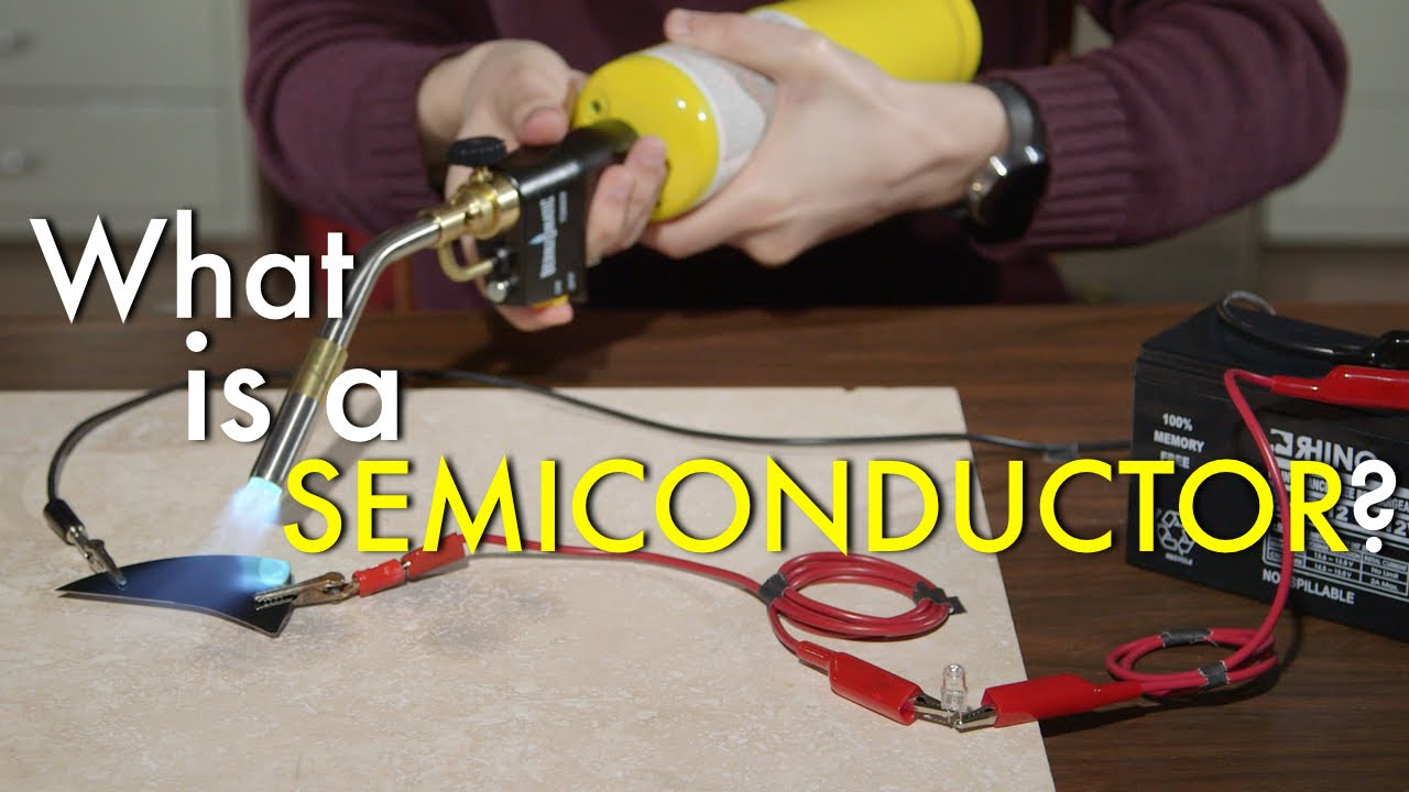
-Semiconductors are crucial because they form the foundation of modern electronics, such as diodes, transistors, microprocessors, solar panels, and digital imaging devices like cameras.
What material is most commonly used for semiconductors, and why?
-Silicon is the most commonly used material for semiconductors because of its unique crystalline structure and its ability to be doped to create both p-type and n-type materials, essential for forming PN junctions.
How does the atomic structure of silicon contribute to its properties as a semiconductor?
-Silicon has a crystalline structure where each silicon atom forms four covalent bonds. This bonding allows for the free movement and vibration of electrons, which is essential for semiconductor behavior, particularly in the formation of PN junctions.
What is doping in the context of semiconductors?
-Doping is the process of adding impurities to silicon to alter its electrical properties. This can involve adding atoms that require more or fewer bonds than silicon, creating p-type (positive) or n-type (negative) materials.
What is the difference between p-type and n-type materials?
-P-type materials have a deficit of electrons, creating 'holes' that require electrons to fill them, while n-type materials have an excess of electrons, making them negatively charged. Together, they form a PN junction.
What is the depletion region in a PN junction?
-The depletion region is the area where p-type and n-type materials meet, and it forms due to the diffusion of electrons and holes. This region has no free electrons and thus has high resistance, preventing current flow.
How do diffusion and drift affect the behavior of a PN junction?
-Diffusion encourages the movement of electrons to form new bonds, while drift resists this movement, aiming to retain the electrons. These opposing forces determine the size of the depletion region and affect the junction's conductivity.
What happens when a PN junction is forward biased?
-When a PN junction is forward biased, the positive end of a power supply is connected to the p-type region and the negative end to the n-type region. This reduces the depletion region and allows current to flow as the resistance decreases.
What is the activation voltage in a diode, and why is it important?
-The activation voltage, typically around 0.6 to 0.7 volts, is the minimum voltage required to collapse the depletion region in a diode, allowing current to flow. Below this voltage, the depletion region remains large, and no current passes through.
Outlines

This section is available to paid users only. Please upgrade to access this part.
Upgrade NowMindmap

This section is available to paid users only. Please upgrade to access this part.
Upgrade NowKeywords

This section is available to paid users only. Please upgrade to access this part.
Upgrade NowHighlights

This section is available to paid users only. Please upgrade to access this part.
Upgrade NowTranscripts

This section is available to paid users only. Please upgrade to access this part.
Upgrade Now


5.0 / 5 (0 votes)