Working of Transistors
Summary
TLDRThis lecture delves into the functioning of bipolar junction transistors (BJTs), highlighting their three-terminal nature and the significance of both electrons and holes in their operation. The video explains the active mode of BJTs, detailing how forward and reverse biases affect the resistance and current flow. It emphasizes the transistor's amplification capability, demonstrating how a weak input signal can be transformed into a stronger output. The script also discusses the movement of charge carriers, the role of barrier potential, and introduces the concept of reverse saturation current. The lecture concludes with a foundational understanding of the relationships between emitter, base, and collector currents in an NPN transistor.
Takeaways
- 😀 The lecture discusses the functioning of a Bipolar Junction Transistor (BJT), emphasizing its role in electronics.
- 🔬 The term 'BJT' stands for Bipolar Junction Transistor, highlighting the involvement of both electrons and holes as charge carriers.
- 🔋 The 'transistor' name is derived from 'transferred resistor,' referring to its ability to transfer a low resistance to a high resistance.
- 📡 In active mode, a BJT operates with one junction (J1) forward-biased and the other (J2) reverse-biased, affecting resistance levels.
- 🔌 The input voltage (VI) is measured across the low resistance, while the output voltage (VO) is across the high resistance, facilitating signal amplification.
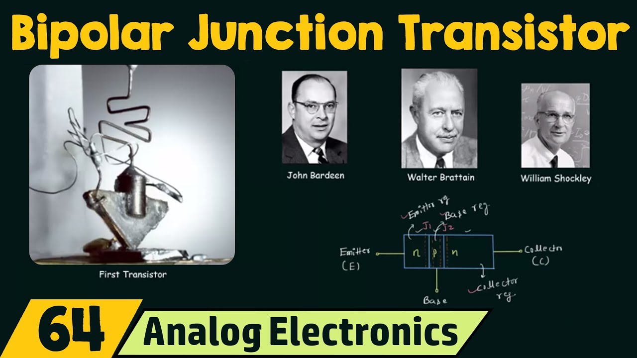
- 🌐 The NPN transistor consists of an n-type emitter, a p-type base, and an n-type collector, with specific terminals for each.
- 🔄 To operate in active mode, the emitter-base junction (J1) must be forward-biased, and the base-collector junction (J2) must be reverse-biased.
- ⚡ The barrier potential at J1 decreases with forward bias, allowing electrons to cross from emitter to base and then to the collector.
- 🔝 Most electrons from the emitter bypass the base due to its thin and lightly doped nature, leading to a significant electron flow to the collector.
- 🔗 The collector current (IC) is primarily determined by the emitter current (IE) and a small reverse saturation current (Ico), with a relationship defined by the transistor's alpha (α).
Q & A
What does BJT stand for?
-BJT stands for Bipolar Junction Transistor. It is called bipolar because it involves both types of charge carriers: electrons and holes.
What is the significance of the term 'transistor'?
-The term 'transistor' is derived from 'transferred resistor'. It refers to the ability of the device to transfer a low resistance to a high resistance, which is key to its amplifying function.
How does the transistor achieve amplification?
-Amplification is achieved by having a weak input signal across a low resistance and an amplified output signal across a higher resistance, with the same current flowing through both.
What is the composition of an NPN transistor?
-An NPN transistor consists of an 'n' emitter region, a 'p' base region, and an 'n' collector region, with corresponding terminals for each.
What is the condition for operating an NPN transistor in active mode?
-For an NPN transistor to operate in active mode, the Junction J1 must be forward biased, and Junction J2 must be reverse biased.
What happens to the barrier potential when a transistor is forward biased?
-When a transistor is forward biased, the barrier potential at Junction J1 is reduced, allowing electrons to cross over from the emitter to the base.
Why does most of the electron flow go to the collector instead of recombining in the base?
-Most of the electrons go to the collector because the base is very thin, lightly doped, and small, which results in minimal recombination of electrons with holes in the base.
What is the significance of alpha (α) in the context of a transistor?
-Alpha (α) represents the ratio of electrons that are collected by the collector to the number of electrons that enter the base. It is a key parameter in determining the transistor's amplification capability.
What is the reverse saturation current and why is it important?
-The reverse saturation current is the current that flows through Junction J2 when it is reverse biased. It is important because it represents the leakage current and is associated with the collector, denoted as IC_o.
How is the collector current (IC) related to the emitter current (IE) and the base current (IB)?
-According to Kirchhoff's current law, the emitter current (IE) is equal to the sum of the base current (IB) and the collector current (IC), expressed as IE = IB + IC.
How does the direction of current relate to the movement of electrons in a transistor?
-The direction of current is opposite to the movement of electrons. For example, in an NPN transistor, emitter current flows from right to left, while electrons move from left to right.
Outlines
🔬 Introduction to Transistors and BJT
This paragraph introduces the concept of transistors, specifically Bipolar Junction Transistors (BJT). It explains the significance of the term 'bipolar' due to the involvement of both electrons and holes as charge carriers. The paragraph also details the meaning behind 'transistor', derived from 'transferred resistor', highlighting the transistor's ability to transfer a signal from a low to a high resistance, thus amplifying the signal. The explanation includes the active mode of operation where one junction is forward-biased and the other is reverse-biased, leading to the amplification of the input signal at the output. The paragraph concludes with an introduction to the NPN transistor, describing its structure and the need to bias it correctly for operation.
🔍 Detailed Analysis of Transistor Biasing
The second paragraph delves deeper into the biasing of transistors, particularly focusing on the barrier potentials at Junction J1 and Junction J2. It discusses how forward biasing reduces the barrier potential at J1, allowing electrons to move from the emitter to the base and then to the collector. The paragraph emphasizes the thin and lightly doped nature of the base, which results in minimal recombination of electrons and holes, leading to a high electron transfer to the collector. It also introduces the concept of reverse saturation current or leakage current, which occurs when Junction J2 is reverse-biased. The paragraph concludes with a discussion of the movement of electrons and the resulting current flow, setting the stage for understanding the transistor's behavior in an electrical circuit.
🔗 Understanding Current Relations in a Transistor
The final paragraph focuses on the relationships between the emitter current (Ie), base current (Ib), and collector current (Ic) in an NPN transistor. It begins by establishing the direction of these currents based on the movement of electrons. The paragraph then uses Kirchhoff's Current Law (KCL) to establish the relationship Ie = Ib + Ic, which is crucial for understanding how current flows within the transistor. The discussion concludes with the formula for the collector current, Ic = α * Ie + Ico, where α represents the efficiency of electron transfer from the emitter to the collector, and Ico is the reverse saturation current. This paragraph provides a foundation for further exploration of transistor behavior and its applications in amplification and other electronic functions.
Mindmap
Keywords
💡Transistor
💡BJT
💡Active Mode
💡Forward Bias
💡Reverse Bias
💡Emitter
💡Base
💡Collector
💡Alpha (α)
💡Kirchhoff's Current Law (KCL)
💡Amplification
Highlights
Explanation of how a transistor works, focusing on its bipolar nature involving both electrons and holes.
Definition of BJT, where B stands for bipolar and J for Junction, indicating two junctions in a transistor.
Origin of the term 'transistor' from 'transferred resistor', highlighting its function in resistance transfer.
Description of active mode operation where one junction is forward biased and the other is reverse biased.
Amplification process using a transistor by comparing input and output voltages across different resistances.
Introduction to the NPN transistor, detailing the roles of the emitter, base, and collector regions.
Procedure to bias the transistor in active mode with forward and reverse bias potentials.
Analysis of electron and hole movement within the transistor due to barrier potential changes.
Importance of the base's thinness and light doping in a transistor, affecting electron recombination.
Explanation of how most electrons from the emitter move to the collector due to high kinetic energy.
Concept of reverse saturation current or leakage current in a reverse-biased junction.
Calculation of collector current as the sum of electrons moving to the collector and the reverse saturation current.
Direction of emitter, base, and collector currents in an NPN transistor, explained with electron movement.
Kirchhoff's current law (KCL) application to determine the relationship between emitter, base, and collector currents.
Emphasis on the significance of alpha in the transistor's operation and its impact on current relationships.
Anticipation of further discussion on alpha in upcoming presentations to deepen understanding of transistor operation.
Transcripts
in the last lecture I introduced
transistors in this lecture I will
explain how transistor works I also
explained the meaning of named BJT BJT B
stands for bipolar B stands for bipolar
we have bipolar in the name because
there is involvement of both type of
charge carriers there is involvement of
electrons as well as holes in transistor
that's why we have bipolar in the name G
stands for Junction J stands for
Junction two junctions are formed in
transistor Junction j1 and Junction j2
two junctions are formed in transistors
so we have Junction in the name now the
most important thing is the meaning of
transistor why we call this three
terminal device transistor the name
transistor is coined from word
transferred resistor transistor is
coined from transferred resistor in
which we have trans
and store I sto R and this two makes the
word transistor now what is the meaning
of transferred resistor if we talk about
active mode if we talk about active mode
of operation then we already know
Junction j1 is forward biased and
Junction j2 is reverse biased when
Junction j1 is forward biased it will
offer a very low resistance or ideally
resistance should be zero when Junction
j2 is reverse biased it will offer a
very high resistance or ideally the
resistance must be infinity so this is
what we have in active mode and if we
have same current same current flowing
then initially it will flow through a
low resistance let's say the current is
I and after this at output it will flow
through high resistance let's say it is
capital R and the same current is
flowing through both these resistances
so somehow we have transferred the low
resistance to the high resistance that's
why we have the name transferred
resistor and from this we got transistor
there is very significant use of this
thing for example let's say VI is the
input voltage and V o is the output
voltage we are measuring VI across this
small resistance and we are measuring vo
across this large resistance so V I is
equal to I multiplied by r and vo is
equal to I multiplied by capital R the
current is same and the input resistance
is smaller than the output resistance so
we can say that VI is smaller than we
owe so we had a weak signal at the input
but we have an amplified signal at the
output so there is amplification
amplification by using the three
terminal device all these things will be
clear when I explain the working of NPN
transistor in active mode this is the
NPN transistor so the emitter region is
n the base region is P and the collector
region is n this is NPN transistor this
terminal is emitter terminal this
terminal is base terminal and this
terminal here is collector terminal and
we want to operate this transistor in
active mode we want to have proper eight
this transistor in active mode and we
already know in active mode Junction j1
is forward bias so two forward bias
Junction j1 we need to we need to apply
a forward bias potential and is
connected to the negative terminal and P
is connected to the positive terminal so
emitter is connected to the negative
terminal and base is connected to the
positive terminal let's say this forward
biasing potential is V EB
and we have to reverse bias Junction j2
so n is connected to the positive
terminal and P is connected to the
negative terminal collector is connected
to the positive terminal base is
connected to the negative terminal and
let's say this reverse biasing potential
is we see B now we have Junction j1
forward biased and Junction j2 reverse
bias now we will analyze the movement of
electrons and holes in this three
terminal device and let's say let's say
VB is the barrier potential for Junction
j1 in Junction j2 when the transistor
terminals are open circuited there is no
biasing potential in the transistor so
VB is the barrier potential for Junction
j1 and Junction j2 when there is no
biasing potential and we have to analyze
what will happen to the barrier
potential once we apply the biasing
potentials in the transistor this is
barrier potential of Junction j2 and it
is equal to VB this is barrier potential
of Junction j1 and it is also equal to
VB now Junction j1 is forward biased
after the application of V EB and the
barrier potential will now reduce and
let's say the new barrier potential is
this the new barrier potential the new
barrier potential is equal to VB VB
minus V EB forward biasing potential on
the other hand Junction j2 is reverse
biased so barrier potential will
increase and the new barrier potential
the new barrier potential is equal to VB
VB plus VC B plus we see be the reverse
biasing potential now we can easily
analyze the movement of electrons and
holes because we have idea about the
barrier potentials because of the
reduced barrier potential at Junction j1
the electrons on the N side that is the
emitter will cross the junction and move
to the base and recombine with the holes
in the base there is one very important
thing
that you always have to keep in your
mind base in case of transistor is very
small it's very small and it is also
lightly lightly domed and because of
this because base is thin and it is
lightly doped there is very small
recombination of electrons from the
emitter and most of the electrons from
the emitter pass over to the collector I
will repeat this point again barrier
potential at Junction j1 is reduced so
electrons from emitter will cross over
the junction and very small amount of
electrons from the emitter will
recombine in the base because base is
very small very thin and it is lightly
doped so most of the electrons will
cross the junction j2 because they have
high velocity and this implies they have
high kinetic energy so most of the
electrons emitted by the emitter will
find themselves in the collector a very
few electrons very few electrons will
recombine with the holes and this means
electrons will move to VEB the positive
terminal of the forward biasing
potential let's say n number of
electrons enter the base and number of
electrons enter the base out of which
one minus alpha n out of which one minus
alpha n electrons combined with the
holes in the base and alpha n alpha and
electrons move to the collector this is
what is happening in the transistor only
2 to 5% 2 to 5% electrons are combined
in the base and 95 to 98% electrons are
collected in the collector therefore
most of the electrons emitted by the
emitter moved to the collector so this
is what will happen when you forward
bias the junction j1 and junction j2 in
bipolar Junction transistor there is one
more thing
that we must not forget and it is the
reverse saturation current Junction j2
is reverse biased so there must be
reverse saturation current through
Junction j2 we have minority charge
carriers on n side and we have minority
charge carriers on P side on n side
minority charge carrier is hole on P
side minority charge carrier is electron
so this hole will move like this and
this electron will move like this so
there there is current called as a
reverse saturation current or leakage
current when the junction j2 is reverse
biased I am calling the reverse
saturation current reverse saturation
current or leakage current or leakage
current IC o---- because this current is
associated with the collector so there
is subscript C this o stands for open
circuit we measure this current when
emitter terminal when ammeter terminal
is open circuited so this is why I am
calling this current IC o---- and if I
if I want to find out the collector
current IC then it is equal to alpha I
alpha times the emitter current because
n is the number of electrons entering
the base and alpha n is the number of
electrons moving to the collector so
current will be alpha times ie plus IC
o---- so this is the value of collector
current the next thing is to find out
relation between the emitter current
base current and collector current for
this purpose first we have to find out
direction of the three currents you can
see electron is moving from left to
right so direction of current is like
this from right to left
this is i.e the emitter current when
electrons from emitter recombine with
the holes the direction of current will
be like this and the current is IB
because electron will move in this
direction to the positive terminal of
the battery so current will
flow in opposite direction and to find
out collector current we again have to
focus on the movement of electrons
electrons are moving from base to
collector like this in this fashion so
current will be like this from right to
left and to find out relation between ie
IB and IC we have to use Kirchhoff's
current law KCl and from KCl we know sum
of currents entering is equal to the sum
of currents leaving ie is leaving I II
is leaving IB and IC are entering so ie
is equal to IB plus IC this is what we
have in the NPN transistor in active
mode these two relations are very
important and we will talk more about
alpha in the coming presentations this
is all for this lecture see you in the
next one
5.0 / 5 (0 votes)