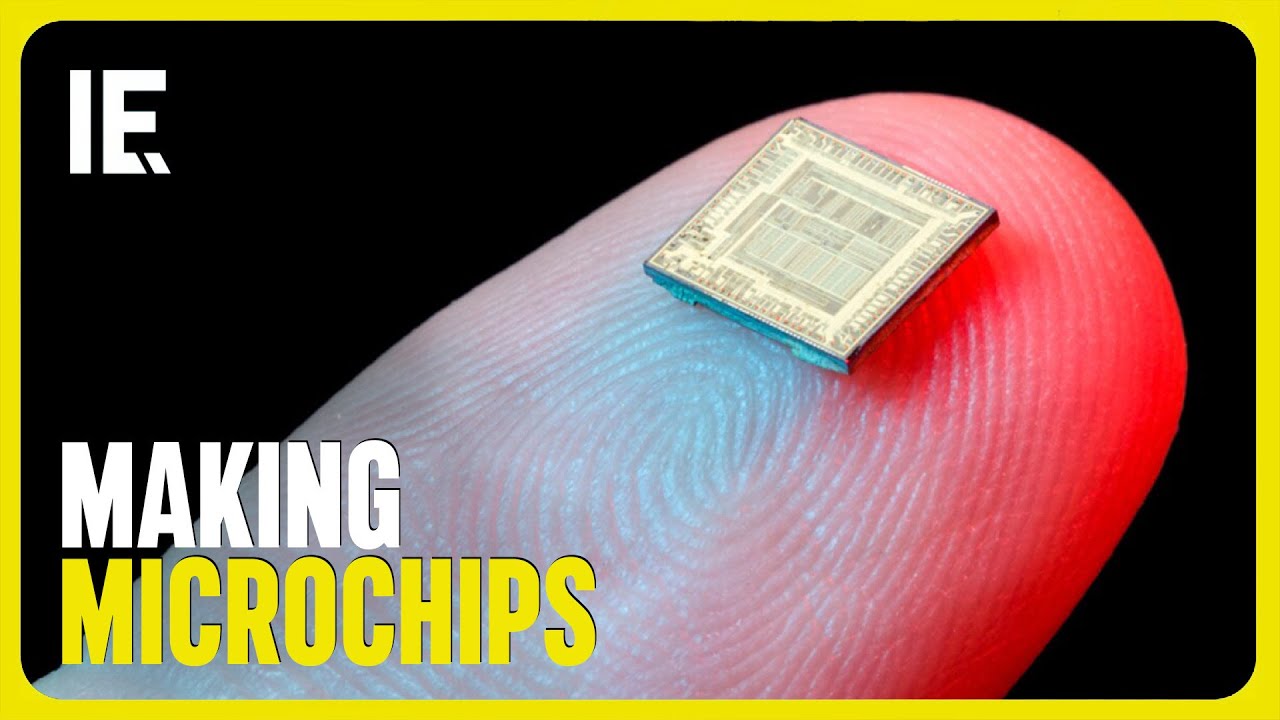
From Sand to Silicon: The Making of a Microchip | Intel
Summary
TLDRThe script delves into Intel's pivotal role in advancing chip technology, highlighting the production process from silicon-rich sand to sophisticated processors. It underscores the innovation in transistor scaling, with breakthroughs like FinFETs and the gate-last fabrication method, enabling high-density contact geometries. The narrative also touches on the importance of packaging technologies in enhancing performance and energy efficiency, showcasing Intel's commitment to driving innovation for smarter, faster, and more connected modern life.
Takeaways
- 🌐 The world is generating data at an unprecedented rate, outpacing our ability to analyze it, highlighting the need for advanced processing power.
- 🚀 Intel is at the forefront of chip manufacturing, creating the backbone of modern electronics with their chips that are integral to various devices and AI technologies.
- 🔬 Intel's manufacturing process is highly innovative, involving the manipulation of atoms to push the boundaries of technology and create groundbreaking products.
- 🔄 The transistor, a tiny switch much smaller than a human hair, is the fundamental component that controls electron flow in circuits, with billions packed into a processor.
- 📈 Intel has consistently doubled transistor density with each new processor generation, a significant achievement in the field of microelectronics.
- 🔩 The process of chip manufacturing begins with melting and cooling silicon-rich sand to form wafers, which are then transformed into chips through a complex sequence of steps.
- 🛠️ Intel's fabrication facilities use automated systems, with wafers traveling long distances between tools for the construction of processors.
- 🏗️ Key steps in the wafer's journey include photolithography, ion implantation, and etching, which set the stage for the critical transistor formation process.
- 💡 Intel pioneered the manufacturing of three-dimensional transistors known as FinFETs, which involve building a channel in the form of a fin to control electron flow.
- 🛑 The 'Gate Last' fabrication method is an Intel innovation that allows for precise placement of dielectric material and metal gate by first constructing and then removing a temporary gate.
- 🔗 Another Intel invention involves moving the transistor contact directly over the active gate, achieved through a novel self-aligning process that facilitates high-density contact geometries.
- 🔋 The final stages of chip production include the addition of metal interconnect layers and innovative packaging technologies that enhance performance and energy efficiency.
- 🔍 Rigorous testing ensures that every Intel chip meets high standards of performance and quality before being released into the market.
- 🌟 Intel's integrated design and manufacturing capabilities have been instrumental in driving innovation and impacting nearly every aspect of modern life.
Q & A
What is the current challenge with the rate of data production compared to our ability to process it?
-The world is producing data at an unprecedented rate, faster than our ability to analyze and understand it, which requires significant processing power.
What role do Intel chips play in modern electronics?
-Intel chips are at the heart of nearly everything within modern electronics, providing the processing power necessary for various devices and AI applications.
What is a transistor and why is it important in chip manufacturing?
-A transistor is a tiny switch that controls the flow of electrons through a circuit. It is crucial as billions of transistors are packed into processors, making it one of mankind's most complex achievements.
How has Intel managed to increase the density of transistors in their processors?
-Intel has essentially doubled transistor density in every new generation of processors by pushing the limits of science and innovation.
What is the starting material for creating silicon wafers used in chip manufacturing?
-The process begins with silicon-rich sand, which is melted and cooled to form a solid that is then sliced into wafers.
What is the role of FOUPs in Intel's manufacturing process?
-FOUPs, or Front Opening Unified Pods, are used to transport raw wafers through Intel's automated system, moving them from tool to tool during the processor construction.
What is photolithography and why is it important in chip manufacturing?
-Photolithography is a process used to transfer a pattern onto the wafer, which is an important step in preparing the wafer for the critical transistor formation process.
What are FinFETs and why were they a breakthrough in transistor manufacturing?
-FinFETs are three-dimensional transistors that allow the gate to wrap around the fin, controlling electron flow more effectively. They represent a breakthrough as they enable continued transistor scaling.
What is the 'gate last' fabrication method and how does it benefit the manufacturing process?
-The 'gate last' method involves building and then removing a temporary gate to precisely place the dielectric material and metal gate, allowing for better control of electron flow in the channel.
How does Intel's self-aligning process for transistor contacts contribute to high-density contact geometries?
-The self-aligning process moves the transistor contact directly over the active gate by recessing and filling the gate material with insulating dielectric, allowing for higher density contact geometries.
What is the significance of innovative processor packaging in advanced computing architecture?
-Innovative processor packaging, including 2D and 3D packaging technologies, is critical as it enables new device form factors and boosts performance and energy efficiency.
How does Intel ensure the quality and performance of their final product?
-Intel conducts thorough testing of the final product to ensure that every chip meets their performance and quality standards.
Outlines
🚀 Data Overload and Intel's Role in Processing Power
The script opens with an acknowledgment of the world's rapid data production, which outpaces our ability to analyze it. It highlights the need for immense processing power to manage this data, from device speeds to AI advancements. Intel is portrayed as a key player in this arena, building chips that are integral to modern electronics. The script introduces the concept of transistors, tiny switches that control electron flow, and discusses Intel's role in doubling transistor density with each new processor generation. The manufacturing process begins with silicon-rich sand, leading to the creation of wafers, which then undergo a complex journey in Intel's facilities.
🔬 The Art of Transistor Fabrication and Innovation at Intel
This paragraph delves into the intricate process of transistor formation within Intel's manufacturing facilities. It describes the initial steps of the wafer's journey, including photolithography, ion implantation, and etching, which prepare the wafer for transistor creation. Intel's pioneering of 3D transistors, known as FinFETs, is emphasized, along with the innovative 'gate last' fabrication method that allows for precise placement of dielectric material and metal gate around the fin. The paragraph also covers another invention that facilitates the direct placement of the transistor contact over the active gate, enhancing the density and performance of the chips.
🔩 Advanced Interconnect Technologies and Packaging Innovations
The script continues by detailing the final stages of the wafer's transformation into a functional processor. It explains the selective etching of dielectrics to expose parts for connection to metal lines, achieved through an innovative via etch and deposition process. The addition of metal interconnect lines completes the circuit, leading to the singulation and packaging of the wafers. The importance of innovative packaging technologies in computing architecture is underscored, with 2D and 3D packaging enabling new device form factors and performance improvements. The paragraph concludes with the testing of the final product to ensure it meets Intel's performance and quality standards.
Mindmap
Keywords
💡Data
💡Processing Power
💡Intel
💡Transistor
💡FinFET
💡Gate Last
💡Dielectric Material
💡Interconnect
💡Singulation
💡Packaging
💡Innovation
Highlights
The world is producing data at an unprecedented rate, faster than our ability to analyze and understand it.
Intel builds chips that are at the heart of nearly everything, from devices to AI.
Innovators are pushing the limits of science, rearranging atoms to create groundbreaking technology.
The transistor, a tiny switch 10,000 times smaller than a human hair, controls the flow of electrons through a circuit.
Intel has doubled transistor density in every new generation of processors.
Silicon-rich sand is melted and cooled to form a solid, which is then sliced into wafers.
Wafers go through a complex process inside Intel fabs, including photolithography, ion implantation, and etching.
Intel was the first to manufacture three-dimensional transistors called FinFETs.
Gate-last fabrication method allows for precise placement of dielectric material and metal gate.
Transistor contact is moved directly over the active gate to enhance performance.
Intel's innovations enable high-density contact geometries through a self-aligning process.
Dozens of layers of metal interconnect lines are added to complete the circuit.
Innovative processor packaging has become a critical feature of advanced computing architecture.
2D and 3D packaging technologies enable new device form factors and boosts in performance and energy efficiency.
Testing of the final product ensures every chip exceeds performance and quality standards.
Intel's integrated design and manufacturing capabilities enable humanity to innovate game-changing technologies.
Intel powers the world, driven by the makers, dreamers, doers, and people who share in making the world smarter, faster, and more connected.
Transcripts
[Music]
the world is producing data
at an unprecedented rate faster than our
ability to analyze and understand it
to move store and compute all of this
data requires incredible processing
power
from the blazing speeds of our devices
to blazing trails within ai
intel builds chips that are at the heart
of nearly everything
within every intel chip manufacturing
facility across the globe
innovators are pushing the limits of
science and literally rearranging atoms
to create
groundbreaking technology this strong
silicon foundation is what gives each
intel chip limitless potential at the
heart of all modern electronics
the transistor is a tiny switch 10 000
times smaller than a human hair that
controls the flow of electrons through a
circuit
to build a processor billions of
transistors
are packed into an area no larger than a
fingernail
it's one of mankind's most complex feats
and a remarkable achievement that intel
has essentially doubled transistor
density
in every new generation of processors
the process begins when silicon-rich
sand is melted and cooled
forming a solid which is then sliced
into wafers
once inside an intel fab the raw wafers
begin their long journey
through an incredibly complex process
they're loaded into front opening
unified
pods or foops which travel hundreds of
miles along intel's automated super
highway
going from tool to tool as processors
are painstakingly built up
on each wafer the wafer first goes
through a series of important steps
such as photolithography ion
implantation
and etching that prepare it for the
critical transistor formation process
intel was the first to manufacture
three-dimensional transistors called
finfets finfet construction requires
first building a channel in the form of
a fin
intel has devised several innovations to
overcome fundamental barriers to
continue transistor scaling
one such innovation is a breakthrough
fabrication method called
gate last it involves building then
removing
a temporary gate in order to precisely
place the dielectric material
and metal gate this allows for the gate
to wrap around the fin
and control the flow of electrons
through the channel
another invention moves the transistor
contact
directly over the active gate to
accomplish this
the gate material is recessed and then
filled with insulating dielectric
material
to prevent the creation of a short
circuit next
the dielectric near the gate is etched
filled with metal recessed
and capped to allow a novel
self-aligning process
that enables the high density contact
geometries
now the dielectrics are etched
selectively to expose
only the desired part to connect to the
first metal lines
this is done through an innovative via
etch and deposition scheme
allowing contact over active gate to
happen
finally dozens of layers of metal
interconnect lines
are added to complete the circuit
after more than a thousand of these
complex steps the wafers are finally
prepared for singulation
and packaging innovative processor
packaging has become a critical feature
of advanced computing architecture
2d and 3d packaging technologies are
enabling new device
form factors and additional boosts in
performance and energy efficiency
testing of the final product ensures
that every chip
exceeds our performance and quality
standards
in addition to adding more performance
and features with each new processor
generation
intel's integrated design and
manufacturing capabilities
have enabled humanity to innovate
game-changing technologies
that impact nearly every facet of modern
life
intel keeps powering the world at the
same time
we're powered by you the makers the
dreamers
the doers the people who share in our
history of making the world smarter
faster and more connected
you
浏览更多相关视频
Modern Onion Farming Technology: How to Process TONS of Onions in Factory
Intel Announces Crazy Plan For AI Chip, That Changes Everything For Nvidia & AMD, 1000 Times Better
Química - Documentário Completo
SMIC making a 3nm Chip for Huawei | China Semiconductor | Space Tech & Military Innovation AI
Microsoft BOMBSHELL Announcements: Sam Altman on GPT-5, Devin Joins Microsoft and Phi-3 (SUPERCUT)
💻 How Are Microchips Made?
5.0 / 5 (0 votes)