Forward Bias (P N Junction Diode) Diode theory & applications (Basic Electronics)
Summary
TLDRThis video lecture introduces basic electronics, focusing on PN junction diodes. The instructor emphasizes the importance of taking notes for effective learning and addresses students' previous requests for updated content. The session explores key concepts such as charge carriers, diffusion current, depletion layers, and potential barriers. It explains how these principles affect current flow in diodes when connected to a power source. The video aims to provide a comprehensive understanding of diode operation, including forward bias connections and the significance of overcoming potential barriers to allow current to flow.
Takeaways
- 😀 The session is focused on basic electronics, specifically the PN junction diode.
- 📚 Students are encouraged to take notes during the video to avoid wasting time later on revisiting concepts.
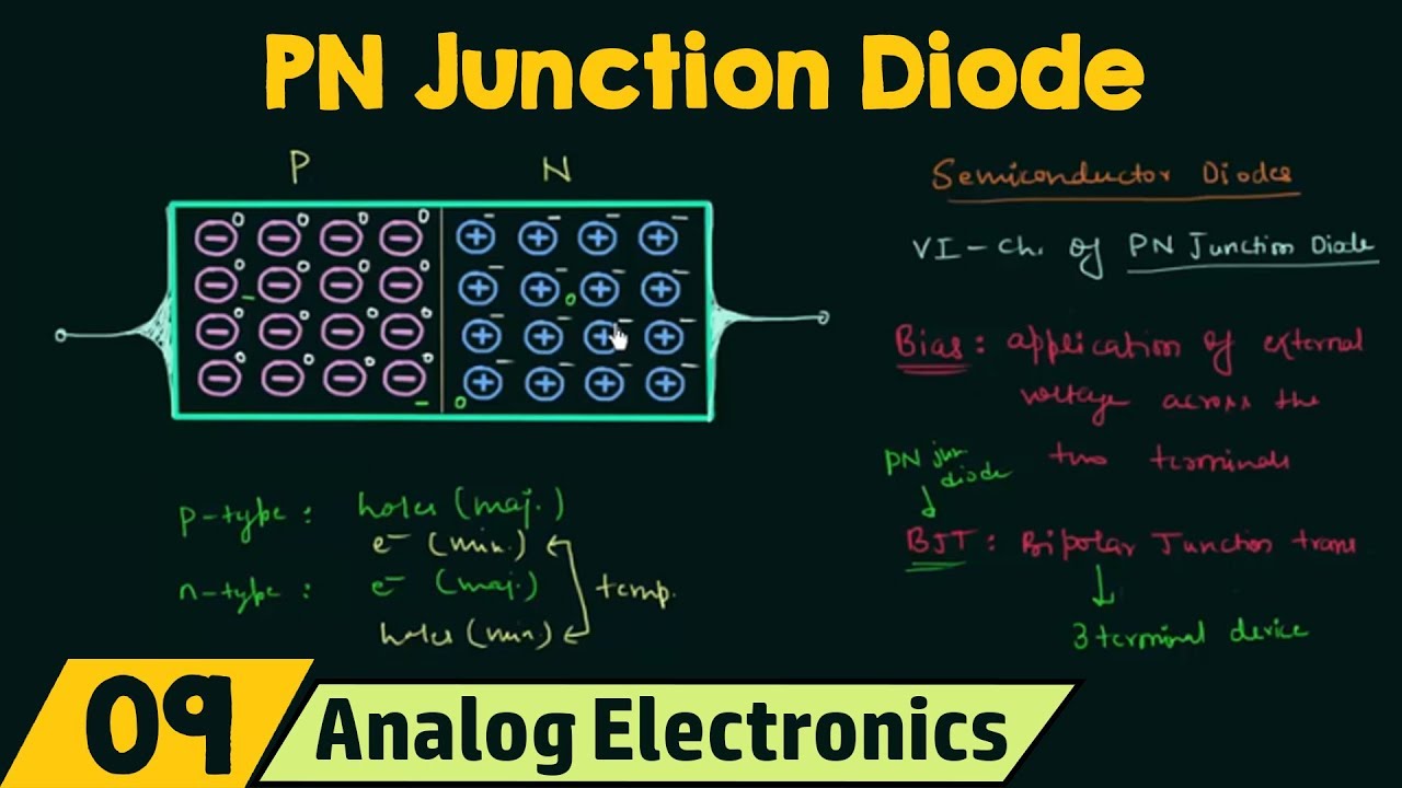
- ⚡ The explanation begins with the definition and functioning of a PN junction diode, describing how it is formed by joining two types of semiconductors.
- 🔌 Current flow in the diode is explained through the movement of electrons and holes, emphasizing the importance of diffusion current.
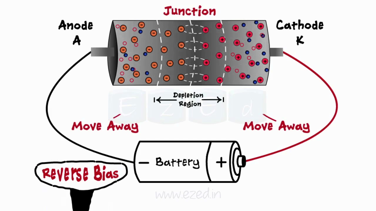
- 🔄 The concept of a depletion layer is introduced, highlighting its role in creating a potential barrier that affects current flow.
- 🔋 When a battery is connected to the diode, it can be in forward or reverse bias, influencing the behavior of the current.
- 🛑 The forward bias condition decreases the depletion layer, allowing current to flow easily, whereas reverse bias increases it, preventing current flow.
- 📏 The thickness of the depletion layer and the electric field within it are crucial for understanding how diodes operate.
- 🔎 The significance of potential barriers is discussed, with specific voltage values (0.6V for silicon) that affect current flow through the diode.
- 📈 The characteristics of the diode are summarized, including the relationship between forward voltage and current flow.
Q & A
What is the main subject being introduced in the video?
-The main subject introduced in the video is Basic Electronics, specifically focusing on the PN Junction Diode.
What preparation is suggested for viewers before watching the video?
-Viewers are advised to have a pen and paper ready to take notes while watching the video to avoid wasting time later on.
What does the term 'diffusion current' refer to in the context of semiconductors?
-Diffusion current refers to the flow of charge carriers (electrons) in a semiconductor, which occurs due to their motion from regions of high concentration to low concentration.
What happens at the depletion layer in a PN junction?
-At the depletion layer, there is a shortage of charge carriers (electrons and holes), leading to a neutral region where no current flows unless a sufficient external voltage is applied.
How is the potential barrier related to the flow of current in a PN junction?
-The potential barrier inhibits the flow of current; it can only be overcome if the applied voltage exceeds this barrier, allowing current to flow.
What is the significance of the potential barrier value mentioned in the video?
-The potential barrier values mentioned are approximately 0.6 to 0.7 volts for silicon, which must be exceeded for current to flow through the diode.
What occurs during forward biasing of a PN junction diode?
-During forward biasing, the positive terminal of a battery is connected to the P-type semiconductor and the negative to the N-type, reducing the depletion layer and allowing current to flow.
What are the characteristics of the current-voltage relationship in a PN junction?
-The current-voltage relationship exhibits a threshold behavior where the current starts to flow significantly only after surpassing the potential barrier.
What role do electric fields play in the operation of a PN junction diode?
-Electric fields influence the movement of charge carriers; in the depletion layer, they create a potential that must be overcome for current to flow.
How can one visualize the symbol of a PN junction diode?
-The symbol of a PN junction diode consists of a triangle pointing towards a line, representing the direction of current flow from the P-side (anode) to the N-side (cathode).
Outlines

This section is available to paid users only. Please upgrade to access this part.
Upgrade NowMindmap

This section is available to paid users only. Please upgrade to access this part.
Upgrade NowKeywords

This section is available to paid users only. Please upgrade to access this part.
Upgrade NowHighlights

This section is available to paid users only. Please upgrade to access this part.
Upgrade NowTranscripts

This section is available to paid users only. Please upgrade to access this part.
Upgrade NowBrowse More Related Video

PN Junction Diode (No Applied Bias)

LED light Emitting Diode (Unit 3 Special purpose diode and Transistors) in हिन्दी

Lab 4 and 5: PN junctions and Solar Cells

Diodes - What Are Diodes - PN Junction - Forward Bias - Reverse Bias - Zener Diodes

Semiconductor PN Junctions, The Depletion Region and Diode Characteristics

Varactor (Construction & Working) Special Purpose Diode (Basic Electronics) BE/BTech 1st year
5.0 / 5 (0 votes)