Barrier Potential
Summary
TLDRThis lecture covers the concept of the built-in potential or barrier potential in a PN junction diode without an applied bias. It explains how diffusion leads to the formation of a depletion layer, which acts as a barrier for further charge movement. The lecture introduces the formula for calculating the barrier potential (V_B = V_T * ln(Na * Nd / Ni^2)), where V_T is the thermal voltage, Na and Nd are acceptor and donor concentrations, and Ni is the intrinsic carrier density. The Boltzmann constant, temperature conversion to Kelvin, and the charge of an electron are also discussed. A numerical example calculates the built-in potential for a silicon PN junction at room temperature.
Takeaways
- ๐ The built-in potential, also known as barrier potential, is the potential difference created at a PN junction with no applied bias.
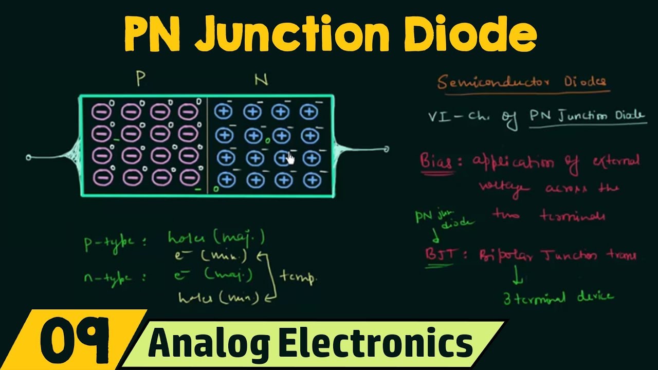
- ๐ Diffusion is the process where free charge carriers recombine, leading to the formation of a depletion layer depleted of free charge carriers.
- ๐ The depletion layer consists of fixed immobile ions with positive and negative charges, which create the barrier potential.
- ๐ซ The barrier potential acts as a barrier to the further movement of charge, preventing the recombination of holes and electrons.
- ๐ The expression for barrier potential (V_B) is given by V_B = V_T * ln((n_a * n_d) / ni^2), where V_T is the thermal voltage.
- ๐ฌ Boltzmann's constant (K) is 1.38066 ร 10^-23 J/K, used to calculate the thermal voltage (V_T).
- โ๏ธ Absolute temperature (T) is in Kelvin, calculated by adding 273 to the temperature in degrees Celsius.
- โก The charge of one electron (e) is 1.6 ร 10^-19 coulombs, used in the calculation of V_T.
- ๐ข At room temperature (27ยฐC or 300K), the thermal voltage (V_T) is approximately 0.026 volts.
- ๐ For a silicon PN junction at room temperature, the barrier potential is approximately 0.757 volts.
- ๐ The barrier potential values for silicon and germanium are often used in semiconductor calculations, with silicon typically at 0.7 volts and germanium at 0.3 volts.
Q & A
What is the built-in potential in a PN junction?
-The built-in potential, also known as barrier potential, is a potential difference that arises at the junction of a PN junction diode due to the diffusion of charge carriers and the formation of a depletion layer. It acts as a barrier to the further movement of charge carriers.
What causes the formation of a depletion layer in a PN junction?
-The depletion layer forms due to the diffusion process where free charge carriers recombine with each other, leading to the creation of immobile ions. This results in a region depleted of mobile charge carriers, leaving behind a layer of fixed immobile ions with opposite charges on the P and N sides.
Why is the depletion layer called so?
-The depletion layer is called so because it is depleted of free charge carriers. It contains only fixed, immobile ions, which are the result of recombination between free charge carriers.
What is the role of the barrier potential in a PN junction?
-The barrier potential acts as a barrier to the further movement of charge carriers. The positive layer on the N side repels electrons, and the negative layer on the P side repels holes, preventing further diffusion and maintaining the potential difference across the junction.
What is the expression for barrier potential (V_B)?
-The expression for barrier potential (V_B) is given by V_B = V_T * ln((n_a * n_d) / ni^2), where V_T is the thermal voltage, n_a is the acceptor concentration, n_d is the donor concentration, and ni is the intrinsic carrier density.
What is the thermal voltage (V_T) and how is it calculated?
-Thermal voltage (V_T) is the voltage equivalent of temperature and is calculated using the formula V_T = (K * T) / e, where K is the Boltzmann constant, T is the absolute temperature in Kelvin, and e is the charge of an electron.
What is the Boltzmann constant and its value?
-The Boltzmann constant (K) is a physical constant that relates the energy at the particle level to temperature. Its value is 1.380649 ร 10^-23 joules per Kelvin.
How do you convert temperature from Celsius to Kelvin?
-To convert temperature from Celsius to Kelvin, you add 273 to the Celsius temperature. For example, 27 degrees Celsius is equal to 300 Kelvin.
What is the charge of an electron?
-The charge of an electron (e) is -1.6 ร 10^-19 coulombs.
How is the built-in potential of a silicon PN junction calculated at room temperature?
-At room temperature (27 degrees Celsius or 300 Kelvin), the built-in potential of a silicon PN junction is calculated using the formula V_B = 0.026 * ln((n_a * n_d) / ni^2), with n_a, n_d, and ni being the acceptor concentration, donor concentration, and intrinsic carrier density, respectively.
What is the typical barrier potential for a silicon PN junction at room temperature?
-The typical barrier potential for a silicon PN junction at room temperature is approximately 0.7 volts.
Outlines
๐ฌ PN Junction Diode and Built-in Potential
The paragraph discusses the concept of a PN junction diode without applied bias, explaining the formation of a depletion layer due to the diffusion of free charge carriers. Diffusion is defined as the recombination of free charge carriers, leading to immobile ions with either positive or negative charges. The depletion layer is formed on the P-side with negative immobile ions and on the N-side with positive immobile ions. This layer acts as a barrier to further charge movement, hence called the barrier potential or built-in potential. The paragraph also introduces the formula for calculating the barrier potential, V_B = V_T * ln((n_a * n_d) / ni^2), where V_T is the thermal voltage, n_a is the acceptor concentration, n_d is the donor concentration, and ni is the intrinsic carrier density. The Boltzmann constant (K) and the charge of an electron (e) are also mentioned as essential components in the formula.
๐ก๏ธ Calculating Thermal Voltage (V_T) and Absolute Temperature
This paragraph elaborates on the calculation of thermal voltage (V_T) using the formula V_T = (K * T) / e, where K is the Boltzmann constant, T is the absolute temperature in Kelvin, and e is the charge of an electron. The paragraph explains how to convert temperature from degrees Celsius to Kelvin by adding 273. The values of K and e are provided, and an example calculation for room temperature (27ยฐC or 300K) results in V_T = 0.026 volts. The importance of using the correct temperature for accurate V_T calculations is emphasized, as changing temperature affects the value of V_T.
๐ Numerical Example of Built-in Potential Calculation
The final paragraph presents a numerical example to calculate the built-in potential (V_B) for a silicon PN junction at room temperature. Given the values for V_T (0.026 volts), acceptor concentration (n_a = 10^16 cm^-3), donor concentration (n_d = 10^16 cm^-3), and intrinsic carrier density (n_i = 1.5 * 10^10 cm^-3), the formula for V_B is applied. The calculation involves taking the natural logarithm of the ratio of the product of acceptor and donor concentrations to the square of the intrinsic carrier density, multiplied by V_T. The result is V_B = 0.757 volts, which represents the barrier potential for a silicon PN junction at room temperature. The paragraph also mentions that similar calculations will be used for other materials like germanium, with different barrier potentials.
Mindmap
Keywords
๐กPN Junction
๐กBuilt-in Potential
๐กDepletion Layer
๐กDiffusion
๐กImmobile Ions
๐กBarrier Potential
๐กThermal Voltage (V_T)
๐กBoltzmann Constant (k or K)
๐กIntrinsic Carrier Density (n_i)
๐กAcceptor Concentration (n_a)
๐กDonor Concentration (n_d)
Highlights
Explanation of PN Junction diode without applied bias
Introduction to built-in potential due to diffusion
Definition of diffusion and its role in PN Junction
Process of recombination of free charge carriers
Explanation of immobile ions acquiring charge
Formation of depletion layer and its characteristics
Role of depletion layer in impeding charge movement
Derivation of the term 'barrier potential'
Expression for barrier potential and its significance
Formula for barrier potential V_B and its components
Explanation of thermal voltage (V_T) and its calculation
Value of Boltzmann constant and its role
Conversion of Celsius temperature to Kelvin
Calculation of absolute temperature from Celsius
Charge of one electron and its significance in V_T
Detailed calculation of V_T at room temperature
General formula for V_T at any temperature
Numerical problem-solving approach for barrier potential
Practical example calculation for silicon PN Junction
Final calculation result for barrier potential at room temperature
Comparison of barrier potentials for silicon and germanium
Conclusion and้ขๅ of next lecture topic
Transcripts
in the last lecture we completed PN
Junction diode with no applied bias I
explained by air potential in the same
lecture and it is also called as
built-in potential built-in potential in
case of no applied bias we do not apply
any external voltage source across these
two terminals and because of diffusion
we have depletion layer because of
diffusion we have depletion layer now
what is diffusion diffusion is the
process in which free charge carriers or
mobile charge carriers recombine with
each other for example for example if we
have immobile ion with hole and if this
hole combines with electron then we have
immobile ion with negative charge on the
other hand if we have immobile ion with
electron and if this electron combines
with hole we have immobile ion with
positive charge now why this immobile
ion is having negative charge on it
whereas this immobile ion is having
positive charge on it because hole this
hole is positively charged and this
immobile ion is losing one hole so it
will have one negative charge on it on
the other hand electron is negatively
charged and this immobile ion is losing
one electron so it will have positive
charge on it and if you see this if you
see the depletion layer you will find on
P side on P side we have layer of
negative immobile ions because whole
combined with electrons and on the N
side we have layer of positively charged
immobile ions because electrons combine
with holes so this is how we get the
depletion layer and it is called as
depletion layer because it is depleted
of free charge carriers we do not have
mobile charge carriers in this reason we
only have fixed immobile ions this whole
process is also called as uncovering of
immobile ions because when we have
immobile ion and hole the charge
neutrality is maintained when we have
mobile ion and electron then also
charged neutrality is maintained but
when whole combines with electron or
electron combines with whole the
uncovering of charge carriers takes
place and we have negatively charged
immobile ion and positively charged a
mobile ion and you can see the layer of
negative immobilize and layer of
positive immobilize act as the potential
difference and this potential difference
is called as barrier potential now why
we are calling it barrier potential
because it is acting as the barrier for
the further movement of charge this
positive layer here will repel the holes
and this negative layer here will repel
the electrons and because of this there
is no further movement of charge
therefore we call it barrier potential
it is also called as built-in potential
and in this lecture we will see the
expression for building potential and we
will also solve one numerical problem on
it so if I draw the built-in potential
or barrier potential then initially it
is zero initially it is zero then it
increases like this and the value the
value is given by V subscript B V
subscript B is barrier potential and we
have to find out the expression for
barrier potential V subscript B and it
is equal to KT by E natural log in
bracket we have na and D upon ni square
so this is the expression for barrier
potential and the derivation is not
important in this course you only have
to remember this formula we will use
this formula to find out barrier
potential this term this term KT by E is
VT VT is the thermal voltage this is
thermal voltage or you can call it
voltage world
age equivalent of temperature and V T is
equal to K T by E we can easily
calculate the value of VT and in
numerical problems we will use the value
of VT directly now what is K K is
Boltzmann constant Boltzmann's constant
and it is equal to one point one point
three eight zero double six multiplied
by 10 raised to power minus 23 joules
per Kelvin so this is the value of
Boltzmann constant and capital T here
capital T here is absolute temperature
absolute temperature and it is in Kelvin
the unit for absolute temperature is
Kelvin and if you have temperature in
degree Celsius if you have temperature
in degree Celsius and you want to
calculate the absolute temperature then
you can easily do it so this is how you
can find the absolute temperature T dash
is the temperature in degree Celsius and
you have to add 273 to it and you will
have your temperature in Kelvin this is
a very basic thing to know for example
for example if temperature is 27 degree
Celsius it means T prime or T dash is
equal to 27 degree Celsius to find out
absolute temperature to find out
absolute temperature
it means capital T it is equal to 273
plus 27 and this will give us 300 Kelvin
so in this way you can find out absolute
temperature the next thing is small e
small a small e is the charge of one
electron charge of electron and it is
equal to it is equal to 1.6
into 10 raised to power minus 19 coulomb
so we are done with the terms involved
in the volts equivalent of temperature
or thermal voltage now we will see what
we have inside this bracket and a and a
is the exception acceptor concentration
and D is donor donor concentration and
Ni and I is intrinsic intrinsic carrier
density so if we have all these things
we can easily calculate the value for VB
that is the barrier potential we will
first calculate the value of V T the
thermal voltage because we will use it
directly in numerical problems it will
save our time so first we will calculate
V T so let's do it quickly VT is equal
to KT by E and let's say the temperature
T - it means the temperature in degree
Celsius is equal to 27 degree Celsius
this is the room temperature this is the
room temperature and as we are
performing the calculations at room
temperature the value of VT is also
valid for room temperature only K is
equal to one point three eight zero
double 6 multiplied by 10 raised to
power minus 23
absolute temperature capital T is equal
to 273 plus 27 and it is equal to 300
Kelvin so we have 300 here and the
charge on one electron is 1.6 into 10
raised to power minus 19 and when you
solve this you will get zero point zero
two six volts so the value of VT is zero
point zero two six and we will use this
directly in numerical problem but there
is one important thing this value of VT
is valid for room temperature only this
is valid
room temperature only because when you
change the temperature when you change
the temperature this number here will
change and the value of VT will also
change but generally you will get
questions in which the temperature is 27
degree Celsius or in question it will be
given calculate the barrier potential at
room temperature in that case we will
take VT equals to zero point zero two
six volts
I will generalize this I will generalize
this for any temperature T dash we will
generalize this T is equal to 273 plus T
dash and this is in Kelvin
VT is equal to K KT by E T is equal to
273 plus T dash so we have 273 plus T
dash I can write this as e by K 273 plus
T dash e by K is 1 point 6 into 10
raised to power minus 19 divided by one
point three eight zero six six
multiplied by 10 raise to power minus 23
and when you solve this when you solve
this you will get 273 plus T dash
divided by one one six double zero so
this is the generalized form of VT and
if it is not the room temperature you
can easily put the value of temperature
here in degree Celsius and you will have
the value of VT so I will modify the
expression I will modify the expression
this expression and V B is equal to VT
natural log in bracket we have n a and D
upon ni square so this is the formula we
will use while solving the numerical
problems let's move to
the numerical problem and this problem
we have to consider a silicon PN
Junction a silicon PN Junction at room
temperature now we have room temperature
so we can say that value of VT is equal
to zero point zero two six volts and it
is doped at na equals to 10 raised to
power 16 per centimeter cube value of n
is equal to 10 raised to power 16 per
centimeter cube and value of nd the
donor concentration is equal to 10
raised to power 17 per centimeter cube
an intrinsic carrier density
it means ni is equal to 1.5 this is 1
point 5 into 10 raised to power 10 per
centimeter cube so n I is equal to 1
point 5 into 10 raised to power 10 per
centimeter cube and we have to calculate
the built-in potential it means we have
to calculate we beam this is very easy
problem we only have to put the values
in the formula so we'll do it quickly VB
is equal to VT natural log in bracket we
have n a nd by ni square VT is equal to
zero point zero two six natural log n a
is equal to 10 raised to power 16 so we
have 10 raised to power 16 multiplied by
10 raised to power 17 and is equal to 10
raised to power 17 and I is 1 point 5
into 10 raised to power 10 so we have 1
point 5 into 10 raised to power 10 whole
square 0.026 natural log 10 raised to
power 16 multiplied by 10 raised to
power 17 is 10 raised to power 33 1
point 5 square
is to point to 5 into 10 raised to power
20 right or we can write it as we can
write it as 0.026 natural log 10 raised
to power 13 10 raise to power 33 divided
by 10 raised to power 20 is equal to 10
raised to power 13 2.25 0.026
when you solve this when you solve this
you will get twenty nine point one two
three after multiplication we have zero
point seven five seven volts and this is
our answer so the barrier potential or
built-in potential is equal to is equal
to zero point seven five seven and this
is for silicon PN Junction at room
temperature and in coming presentations
also I will use barrier potential for
silicon equal to 0.7 volts and barrier
potential for germanium equals to zero
point three volts this is very important
because we will use this a lot this is
important and this is calculated at room
temperature so this is all for this
lecture
in the next lecture we will discuss
width of depletion region we will solve
one numerical problem on width of
depletion region so this is also in the
next one
Browse More Related Video
PN Junction Diode (No Applied Bias)
U1_L2_P-N Junction Diode | Electronics Engineering (BEC101/201)| Hindi
VI Characteristics of PN Junction Diode | PN Junction Forward Bias | PN Junction Reverse Bias
5.1 Forward and reverse biased PN junctions
V-I Characteristics of PN Junction Diode in Hindi | TECH GURUKUL By Dinesh Arya
SCP07: Carrier concentration in intrinsic semiconductor
5.0 / 5 (0 votes)