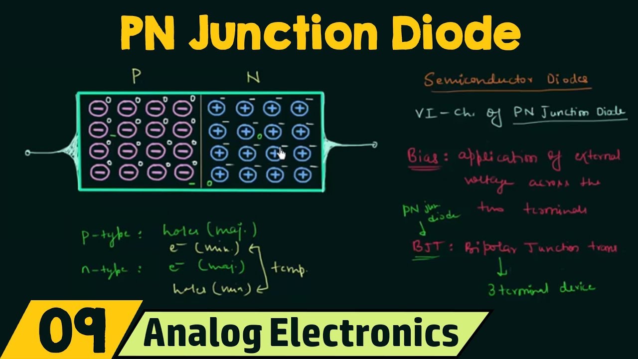
Basic Electronics: PN Junction Working Principle and V-I Characteristics of PN Junction Diode
Summary
TLDRIn this lecture, the formation and working principle of a PN Junction diode are explored. The process begins with the connection of P-type and N-type semiconductors, leading to the formation of the junction. The key concepts discussed include diffusion and drift currents, concentration differences, and the creation of depletion layers. The video covers forward and reverse bias, explaining the behavior of the diode in both cases. Key terms like junction potential, threshold voltage, and avalanche breakdown are explained, along with the characteristics of the diode under different conditions. The session concludes with a discussion of the current-voltage relationship and diode resistance.
Takeaways
- 😀 PN Junction is formed when a P-type semiconductor is connected to an N-type semiconductor, creating a diode.
- 😀 The principle of PN Junction formation is based on the concentration difference between majority and minority charge carriers in P and N semiconductors.
- 😀 Diffusion occurs when majority charge carriers (holes in P and electrons in N) move to balance concentrations, creating immobile charge carriers at the junction.
- 😀 A depletion layer forms as electrons and holes accumulate near the junction, creating a potential barrier known as the junction voltage (Vb).
- 😀 Two types of currents flow in the PN Junction: Diffusion current (from P to N) and Drift current (due to the electric field created in the depletion layer).
- 😀 The direction of diffusion current is from P to N, while the direction of drift current is from N to P.
- 😀 The junction potential is typically 0.7V for silicon and 0.3V for germanium, beyond which the junction barrier breaks down and conduction current flows.
- 😀 In forward bias, the positive terminal of the power supply connects to the P side and the negative terminal to the N side, causing current to flow easily once the threshold voltage is surpassed.
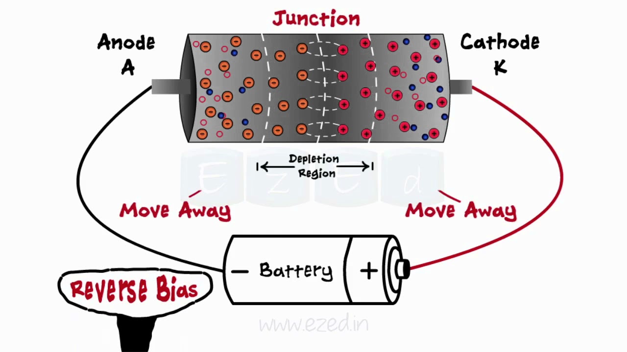
- 😀 In reverse bias, the negative terminal connects to the P side and the positive to the N side, resulting in very little current flow (leakage current) due to the widening of the depletion layer.
- 😀 The reverse bias current increases significantly once the voltage exceeds the avalanche breakdown voltage, leading to a sharp rise in current flow.
- 😀 The voltage-current characteristics of the diode are nonlinear, with forward bias exhibiting an exponential increase in current beyond the threshold voltage and reverse bias showing leakage current until avalanche breakdown occurs.
Q & A
What is a PN Junction and how is it formed?
-A PN Junction is formed when a P-type semiconductor is connected to an N-type semiconductor. The majority charge carriers in P-type are holes, and in N-type, they are electrons. The junction is formed due to the concentration difference between the majority carriers of both semiconductors.
What is the significance of the concentration difference in a PN Junction?
-The concentration difference between the majority charge carriers of the P and N semiconductors causes diffusion. Holes from the P-side diffuse to the N-side, and electrons from the N-side diffuse to the P-side, leading to the formation of a depletion layer.
What is the role of diffusion current in a PN Junction?
-The diffusion current occurs due to the movement of charge carriers across the junction. Holes move from P to N, and electrons move from N to P, creating an imbalance and leading to the formation of immobile ions at the junction, resulting in a depletion region.
What happens when the concentration of charge carriers becomes equal in a PN Junction?
-When the concentration of charge carriers becomes equal, the diffusion process stops. At this point, a junction potential, known as the junction barrier or potential barrier, is established, and an electric field forms within the depletion layer.
What is the difference between diffusion current and drift current in a PN Junction?
-Diffusion current occurs due to the movement of charge carriers from areas of high concentration to low concentration. Drift current, on the other hand, is caused by the electric field that develops within the depletion layer, causing charge carriers to move in a specific direction.
What is the relationship between junction potential and the type of semiconductor material?
-The junction potential depends on the material of the semiconductor. For silicon, the junction potential is typically 0.7V, while for germanium, it is around 0.3V. If the applied voltage exceeds these values, the junction will break down, allowing current to flow.
What is the effect of forward bias on a PN Junction?
-In forward bias, the positive terminal of the power supply is connected to the P-side, and the negative terminal is connected to the N-side. This reduces the width of the depletion region, and if the applied voltage exceeds the threshold voltage (0.7V for silicon), the junction barrier breaks down, allowing current to flow.
What happens during reverse bias in a PN Junction?
-In reverse bias, the positive terminal of the power supply is connected to the P-side, and the negative terminal is connected to the N-side. This increases the width of the depletion region and the potential barrier, causing very little current to flow, known as leakage current. If the reverse voltage exceeds the breakdown voltage (Avalanche or Zener voltage), a large current will suddenly flow.
What is the significance of the knee voltage (threshold voltage) in a PN Junction?
-The knee voltage, or threshold voltage, is the minimum voltage required to forward bias a PN Junction. For silicon, it is 0.7V, and for germanium, it is 0.3V. Once the applied voltage exceeds this value, the depletion region breaks down, and the current starts to increase rapidly.
What is the difference between static resistance and dynamic resistance in a PN Junction?
-Static resistance is the resistance at a specific point on the voltage-current curve, calculated by dividing the voltage by the current (V/I). Dynamic resistance, on the other hand, is the slope of the voltage-current graph and is calculated by the change in voltage (dV) divided by the change in current (dI).
Outlines

This section is available to paid users only. Please upgrade to access this part.
Upgrade NowMindmap

This section is available to paid users only. Please upgrade to access this part.
Upgrade NowKeywords

This section is available to paid users only. Please upgrade to access this part.
Upgrade NowHighlights

This section is available to paid users only. Please upgrade to access this part.
Upgrade NowTranscripts

This section is available to paid users only. Please upgrade to access this part.
Upgrade NowBrowse More Related Video
5.0 / 5 (0 votes)


