Lab 4 and 5: PN junctions and Solar Cells

Shubhadeep Bhattacharjee
30 Aug 202326:11

Summary

TLDRThis video lecture provides a concise overview of PN junction diodes and their operation. It explains the basic concepts of diodes as electronic components that allow current to flow in one direction, akin to a plumbing valve. The lecture revisits the principles of p-type and n-type semiconductors, the formation of depletion regions, and the role of built-in electric fields. It also touches on forward and reverse biasing of diodes, leading to their rectification properties, which are crucial for various semiconductor devices. The lecture concludes with a brief mention of upcoming topics on solar cells.

Takeaways

  • 📘 The lab focuses on experiments with PN junction diodes and solar cells, with a brief theory recap.
  • 🧠 A diode is compared to a one-way valve in plumbing, allowing current to flow in one direction while blocking it in the opposite direction.
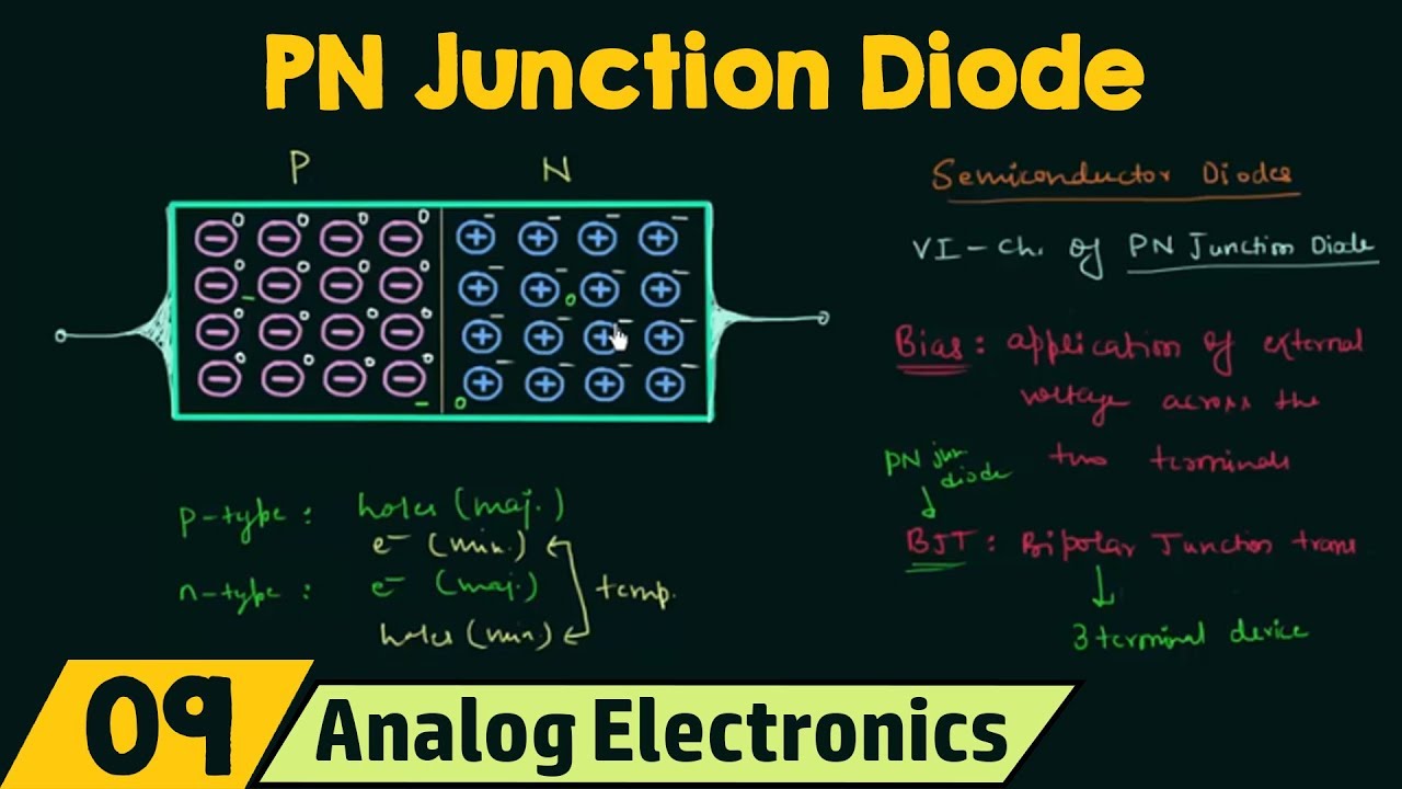
  • ⚙️ A diode is made from p-type and n-type semiconductor materials, typically silicon, which are joined together to form a junction.
  • 🔋 In intrinsic silicon, there are no free electrons, making it an insulator; doping silicon with trivalent or pentavalent atoms turns it into p-type or n-type silicon, respectively.
  • ⚡ P-type silicon has an excess of holes (positive charge carriers), while n-type silicon has an excess of electrons (negative charge carriers).
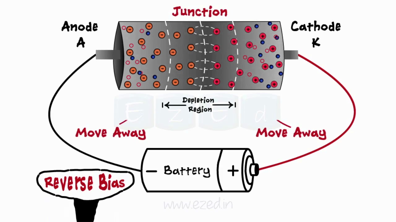
  • 🔄 When p-type and n-type silicon are joined, electrons and holes diffuse across the junction, creating a space charge region or depletion region where no free carriers exist.
  • ⚖️ The built-in electric field created by the separation of charges in the depletion region prevents further diffusion, maintaining equilibrium.
  • ➡️ Applying a forward bias (positive on p-side, negative on n-side) reduces the built-in electric field, allowing current to flow.
  • ⬅️ Applying a reverse bias (negative on p-side, positive on n-side) strengthens the built-in electric field, blocking current flow.
  • 📈 In the forward bias, the current increases exponentially with voltage, while in reverse bias, the current remains negligible and constant.

Q & A

  • What is the primary function of a diode?

    -A diode acts as an electronic switch, allowing current to flow in one direction (forward bias) and blocking current flow in the opposite direction (reverse bias).

  • What happens when a P-type and an N-type semiconductor material are brought into close contact?

    -When a P-type and an N-type semiconductor material are brought into close contact, a PN junction is formed. This junction creates a depletion region where the majority of free charge carriers (electrons and holes) are depleted due to diffusion of electrons from the N-side to the P-side and holes from the P-side to the N-side.

  • Why is silicon commonly used as a semiconductor material?

    -Silicon is commonly used as a semiconductor material because it is a group 4 element with four valence electrons, which allows for the formation of a perfect lattice structure. It can be easily doped to create P-type or N-type semiconductors by adding impurities like boron (trivalent) or phosphorus (pentavalent).

  • How does doping with a trivalent atom like boron create a P-type semiconductor?

    -Doping with a trivalent atom like boron creates a P-type semiconductor because boron has three valence electrons, which leaves an unpaired 'hole' when it bonds with neighboring silicon atoms. This hole can move through the lattice and act like a positively charged entity, thus creating P-type material.

  • What is the role of the built-in electric field in a PN junction?

    -The built-in electric field in a PN junction acts as a barrier to prevent further diffusion of charge carriers (electrons and holes). It is generated due to the separation of charges in the depletion region and helps maintain equilibrium in the system.

  • What is the effect of applying a forward bias to a PN junction diode?

    -Applying a forward bias to a PN junction diode reduces the barrier created by the built-in electric field, allowing current to flow more easily from the P-side to the N-side. This results in an exponential increase in current with increasing voltage.

  • How does reverse bias affect the current flow in a PN junction diode?

    -Applying a reverse bias to a PN junction diode strengthens the built-in electric field, which further prevents the flow of charge carriers. This results in a very small, almost negligible, and constant current flow that does not significantly change with voltage.

  • What is the significance of the depletion region in a PN junction?

    -The depletion region in a PN junction is significant because it is devoid of free charge carriers (electrons and holes). This region is crucial for the diode's rectification property, allowing current to flow in one direction and blocking it in the other.

  • What will be observed during the lab experiment with PN junction diodes?

    -During the lab experiment with PN junction diodes, students will observe the IV characteristics of the diode. In forward bias, they will see an exponential increase in current with voltage, while in reverse bias, the current will remain negligible and almost constant.

  • What is the difference between equilibrium and non-equilibrium conditions in a PN junction?

    -In equilibrium conditions, no external bias is applied, and the system is in a balanced state with a built-in electric field preventing further diffusion of charge carriers. In non-equilibrium conditions, an external bias is applied, which can either counteract (forward bias) or strengthen (reverse bias) the built-in electric field, affecting the flow of current.

Outlines

00:00

🔬 Introduction to PN Junction Diodes and Solar Cells

This paragraph serves as an introduction to the lab session, focusing on experiments with PN junction diodes and solar cells. The speaker briefly revisits the basic theory of these topics, highlighting their importance and explaining that while detailed theory will be covered in a later course, the provided information is sufficient for conducting the experiments.

05:02

🛠️ Basics of Diodes: Electronic Valves

The speaker introduces the concept of a diode, comparing it to a valve in plumbing that controls the direction of flow. In electronics, diodes allow current to flow in one direction (forward bias) while blocking it in the reverse direction. The paragraph emphasizes the importance of diodes in creating controlled circuits and discusses their ideal versus real characteristics, which will be explored in the lab through IV measurements.

10:03

🧪 Understanding P-Type and N-Type Semiconductors

This paragraph explains how doping silicon with trivalent or pentavalent atoms creates P-type and N-type semiconductors, respectively. It describes how replacing a silicon atom with boron introduces holes (P-type), and replacing it with phosphorus introduces free electrons (N-type). The paragraph underscores the maintenance of overall charge neutrality in both types of semiconductors despite the presence of these charge carriers.

15:04

🔄 Diffusion and Space Charge Region in PN Junctions

The focus here is on the diffusion process when P-type and N-type silicon are joined, leading to the formation of a space charge region or depletion region. The speaker explains how holes and electrons diffuse across the junction, resulting in a separation of charges and the creation of an internal electric field. This field opposes further diffusion, stabilizing the junction in equilibrium.

20:07

⚡ Built-In Electric Field and PN Junction Equilibrium

This paragraph discusses the role of the built-in electric field in a PN junction at equilibrium, where no external bias is applied. The electric field, generated by the separation of charges, prevents further diffusion of charge carriers. The speaker sets the stage for discussing non-equilibrium conditions by explaining how the internal electric field maintains the junction's stability.

25:07

🔌 Forward and Reverse Bias in PN Junctions

The speaker explains how applying an external bias affects the PN junction. In forward bias, the external field opposes the built-in field, reducing its effect and allowing current to flow easily. In reverse bias, the external field strengthens the built-in field, further inhibiting the flow of charge carriers. The paragraph outlines how these behaviors lead to the rectifying properties of diodes, with forward bias allowing exponential current increase and reverse bias resulting in minimal current flow.

📝 Summary and Conclusion on PN Junction Diodes

This final paragraph recaps the main points about PN junction diodes, focusing on how the space charge region and built-in electric field create the diode's rectifying behavior. The speaker concludes with a preview of the next lab session, which will cover solar cells, and encourages the audience to understand these foundational concepts before moving forward.

Mindmap

Keywords

💡PN Junction

A PN junction is the boundary between p-type and n-type semiconductor materials. It is a fundamental component in devices like diodes and solar cells. In the video, the PN junction is described as a key structure that enables rectification by allowing current to flow in one direction while blocking it in the opposite direction.

💡Diode

A diode is an electronic component made from a PN junction that allows current to flow in one direction but not in the reverse. In the video, the diode is compared to a one-way valve in plumbing, controlling the direction of current flow based on biasing conditions.

💡Forward Bias

Forward bias refers to the condition where a positive voltage is applied to the p-side of the diode and a negative voltage to the n-side, reducing the barrier and allowing current to flow. The video explains that under forward bias, the internal electric field of the diode is counteracted, leading to increased current flow.

💡Reverse Bias

Reverse bias is the condition where a negative voltage is applied to the p-side and a positive voltage to the n-side of the diode, enhancing the built-in electric field and preventing current flow. The video mentions that in reverse bias, only a very small leakage current flows, demonstrating the diode's rectifying property.

💡Depletion Region

The depletion region is the area around the PN junction that is depleted of free charge carriers (electrons and holes). It forms due to the diffusion of carriers across the junction, creating a region with immobile charged ions. In the video, this region is crucial for the diode's rectifying behavior, as it determines how easily current can flow through the device.

💡Built-in Electric Field

The built-in electric field is an internal field created by the separation of charges in the depletion region of a PN junction. It prevents further diffusion of charge carriers across the junction. In the video, this electric field is fundamental to the functioning of the diode, controlling the flow of current under different biasing conditions.

💡Doping

Doping is the process of intentionally adding impurities to a semiconductor to modify its electrical properties. P-type doping adds elements with fewer valence electrons, creating 'holes,' while n-type doping adds elements with more valence electrons, providing extra electrons. The video describes how doping creates p-type and n-type materials, which form the PN junction.

💡Rectification

Rectification is the process of converting alternating current (AC) to direct current (DC). In the video, the diode's ability to allow current to flow in only one direction under forward bias and block it under reverse bias is highlighted as the basis for rectification in electronic circuits.

💡Semiconductor

A semiconductor is a material with electrical conductivity between that of a conductor and an insulator. The video uses silicon as an example, explaining that its electrical properties can be altered through doping, making it suitable for creating electronic components like diodes and solar cells.

💡Diffusion

Diffusion is the movement of particles from an area of higher concentration to an area of lower concentration. In the context of the video, diffusion describes the movement of electrons and holes across the PN junction, leading to the formation of the depletion region and the built-in electric field.

Highlights

Introduction to lab experiments on PN Junction diodes and solar cells.

Recap of PN Junctions and solar cells theory from 11th and 12th grade studies.

Explanation of a diode as an electronic switch, allowing current flow in one direction.

Description of forward bias and reverse bias in diodes.

Composition of a diode from P-type and N-type semiconductor materials.

The role of doping in creating P-type and N-type semiconductors.

Mechanism of hole and electron movement in PN Junctions.

Formation of the depletion region and its effect on charge carrier movement.

The concept of charge neutrality in PN Junctions despite local charges.

Diffusion of charge carriers and the creation of the space charge region.

The built-in electric field's role in preventing further diffusion of charge carriers.

Equilibrium condition in PN Junctions without external bias.

Impact of forward bias on reducing the built-in electric field and increasing current flow.

Exponential increase in current under forward bias due to reduced internal electric field.

Application of reverse bias and its effect on strengthening the internal electric field.

Negligible current flow in reverse bias due to strengthened internal electric field.

Practical lab measurements of IV characteristics of PN Junction diodes.

Overview of the rectification process in PN Junction diodes.

预告下一周将讲解太阳能电池的更多细节。

Transcripts

play00:01

so hello and welcome to the lab four and

play00:05

five

play00:05

uh in ae2301e2501

play00:10

uh in this particular lab we will be

play00:12

doing a few experiments

play00:14

on PN Junction diodes and solar cells so

play00:19

before we do the experiments it might be

play00:22

worthwhile to

play00:23

recall or revise a little bit of theory

play00:26

and that is what the objective of this

play00:28

short video lecture will be

play00:31

so you might have already studied about

play00:33

PN Junctions and solar cells in your

play00:36

11th and 12th I'll just recap

play00:38

uh the key Concepts whereas you have but

play00:43

please note that your

play00:45

detailed Theory would be covered in your

play00:48

semiconductor device fundamentals course

play00:51

but the stuff that I'm going to discuss

play00:54

today will suffice in helping you do the

play00:57

experiment so let us begin

play00:59

so

play01:00

so we begin with PN Junctions to create

play01:03

these device called diodes

play01:06

so this is the base very basic and most

play01:09

fundamental semiconductor device that

play01:11

you can build in the lab so what is a

play01:14

diode a diode is nothing what I would

play01:17

call is nothing but an electronic wolf

play01:20

right so as you know in your water

play01:23

Plumbing Systems you suppose you have a

play01:26

pipe in most cases you need to build

play01:29

these so-called walls

play01:33

and these walls what their primary

play01:35

functionality is to

play01:37

uh they are built something like this so

play01:40

as you can see the primary functionality

play01:42

of the wall is to allow the flow of

play01:45

water in this direction but to disallow

play01:48

the flow of water in this particular

play01:51

direction right

play01:53

so similarly it is also very important

play01:55

to have diodes which act as electronic

play01:58

words so what what does what the diode

play02:03

essentially does is allows the flow of

play02:05

current so if I draw a corresponding

play02:08

electronic

play02:10

counterpart for a plumbing wall what I

play02:13

would do is I have voltage and I have

play02:16

current so the job of a diode in the

play02:19

forward

play02:21

quadrant or in the first quadrant is to

play02:23

allow the flow of current as you know

play02:26

and in the reverse quadrant is to block

play02:28

the flow of current so this is

play02:31

therefore called forward bias

play02:34

and this is called reverse price right

play02:37

so what we are going to do is try to see

play02:40

that this is your ideal characteristics

play02:43

that you want from a dial

play02:47

but as you know when you start making

play02:49

semiconductor devices hardly anything is

play02:52

ideal so the question that we will try

play02:55

to ask is uh what does an actual

play02:58

semiconductor diode look like

play03:00

so before we ask that question what we

play03:03

will do is and not just ask the question

play03:05

we will also make measurements on a

play03:07

common diode uh which will be given to

play03:10

you in the lab we will make certain IV

play03:12

measurements and see how diodes

play03:14

characteristics looks like

play03:17

but what is a diode made up of so a

play03:19

diode as you know might be as you might

play03:21

know is made up of a b type

play03:24

semiconductor material and an type

play03:27

semiconductor material brought in close

play03:29

content so when a junction is formed

play03:32

between

play03:33

a p-type semitone P type semiconductor

play03:37

let's assume that the semiconductor is

play03:40

is the commonly known silicon and an

play03:43

n-type semiconductor

play03:46

and type silicon when you bring the n t

play03:49

type and N type Semiconductor in this

play03:53

case happens to be silicon the most

play03:55

common semiconductor together

play03:57

you are able to construct or you are

play04:00

able to make a diode okay so how does

play04:04

this work is what we will try to explore

play04:07

right now

play04:13

so let's try to recall what we know or

play04:16

what we understand by P and N type

play04:18

doping uh so as you know silicon

play04:21

is a group 4 element

play04:23

so it has

play04:26

four valence electrons which is bonded

play04:29

to other silicon atoms as well

play04:33

and in its intrinsic Case by intrinsic

play04:36

case I mean that you have a perfect

play04:38

silicon lattice

play04:39

with no impurities this B has more or

play04:43

less like a

play04:44

insulator why because all the electrons

play04:47

are bound to each other and there is no

play04:49

movement of electrons for it to become a

play04:52

conductor as you know how conductors and

play04:54

insulators are distinguished is from the

play04:57

fact that in conductors you have very

play04:59

high conductivity because of presence of

play05:01

free electrons as you can see if you

play05:04

have a

play05:05

perfect lattice of silicon all silicon

play05:08

atoms are bonded uh to neighboring four

play05:12

silicon atoms and therefore there is no

play05:14

presence of any free electrons therefore

play05:17

we can assume that a silicon's perfect

play05:20

lattice will behave more like an

play05:22

insulator and that is what we generally

play05:24

see it's insulin it has very uh High

play05:28

Resistance or very low conductivity so

play05:31

but however we want current to flow

play05:34

through certain system through this

play05:35

particular material and that is what

play05:37

makes semiconductor so special that you

play05:40

can alter or you can dope the material

play05:42

or dope the semiconductor such that it

play05:45

can either conduct electrons or holes

play05:47

right this is what we have been studying

play05:50

in our 11th and 12th standard also so

play05:53

how does that happen what you

play05:55

essentially do is you replace one of the

play05:57

Silicon atoms with a pentavalent atom or

play06:03

a trivalent atom so let's try to do that

play06:05

so if we replace this particular silicon

play06:09

if we delete off this particular silicon

play06:11

and you replace it with a

play06:14

if you replace this with a

play06:16

atom which is you substitution you

play06:20

substitute the silicon atom which was on

play06:22

the right hand side with a trivalent

play06:24

atom such as Boron you will see boron

play06:29

will have three

play06:32

valence electrons only and because boron

play06:35

has three valence electrons it will bond

play06:37

to only three neighboring atoms of

play06:41

silicon right so suppose it goes and

play06:43

bonds with three neighboring atoms of

play06:46

silicon and what you have remaining if

play06:49

you look carefully is this

play06:51

extra electron which is unpaired

play06:55

right and as we were discussing that

play06:57

there is no

play06:59

atom there is no electron from Boron to

play07:02

compensate for this missing

play07:05

one extra electron in the Silicon so

play07:08

what we have in

play07:10

this place is an absence of an electron

play07:12

which is also called a hole

play07:15

and as we know this particular hole can

play07:17

Traverse through the lattice

play07:19

on application of an electric field and

play07:23

act like a like a positively charged

play07:25

entity and therefore we call that this

play07:27

has become a

play07:29

p-type silicon

play07:31

on the other hand if I have the same

play07:34

silicon lattice

play07:39

and I replace one of the silicons

play07:42

with a pentavalent atom

play07:46

pentavalent

play07:49

let's say phosphorus

play07:51

what will happen the phosphorus has five

play07:56

the phosphorus atom has five

play08:00

electrons which will bond to its

play08:03

neighboring silicon atoms

play08:12

and what remains is this extra electron

play08:17

and this extra electron

play08:20

which I will Mark with

play08:22

red

play08:24

can Traverse through the lattice

play08:28

and this extra electron is what gives

play08:31

this silicon

play08:33

just an n-type silicon characteristics

play08:36

so as we just discussed p-type silicon

play08:40

has an excess of holes

play08:43

and the n-type Silicon has an excess of

play08:47

electrons please remember that although

play08:50

you have electrons and holes which are

play08:53

positively uh and negative uh positive

play08:57

negatively and positively charged

play08:59

respectively overall the charge

play09:01

neutrality of the system remains why is

play09:04

that the case because of an electron

play09:06

leaves this particular side and moves

play09:09

around in the lattice and equivalent

play09:11

positive charge is created on the

play09:14

phosphorus atom

play09:15

so please never get confused that n type

play09:18

and p-type silicon atoms are negatively

play09:21

and positively charged yes locally they

play09:23

might have some charge but overall

play09:25

charge neutrality is maintained okay so

play09:28

now that we understand what P type and

play09:30

n-type silicon is or an n-type and

play09:33

p-type semiconductor is let's see what

play09:35

happens when you join both PN and type

play09:38

silicon together

play09:40

so what happens when you join p and N

play09:42

type silicon together is the following

play09:45

so I'm sure you might have studied about

play09:48

this law called the law of diffusion or

play09:51

the fixed law

play09:56

remember what the fixed law used to tell

play09:58

you which was nothing but the law of

play10:00

diffusion

play10:02

it just says that

play10:05

if there is some

play10:07

quantity which can move around in space

play10:09

a best example to give is probably a gas

play10:12

molecule if a gas molecule can move

play10:15

around its space and you have a high you

play10:18

open a bottle which has a high

play10:19

concentration of this particular gas

play10:21

molecule it could be a perfume it will

play10:23

diffuse into space what does that mean

play10:26

that it will move from region of

play10:30

higher concentration to a area of lower

play10:34

concentration and this is what exactly

play10:36

happens when you join an p and n-type

play10:39

silica material together so please

play10:41

recall you had P silicon and N silicon

play10:44

and when you the P silicon had an excess

play10:47

of holes

play10:49

which I'm marking with red and the N

play10:53

silicon had an excess of electrons

play10:56

which I am marking with green

play11:00

so if there are excess of electrons and

play11:02

holes what essentially will happen if

play11:05

electrons will move or diffuse from the

play11:09

n-type Silicon to the p-type Silicon

play11:12

and

play11:14

holes will move from p-type Silicon to

play11:18

n-type Silicon right

play11:20

so this diffusion will happen because

play11:23

holes are higher in concentration and B

play11:26

side compared to enzyme and electrons

play11:28

are in higher concentration in inside

play11:31

compared to the P side this is very

play11:33

simple but the question we ask is will

play11:35

this diffusion

play11:37

happen continuously or there will be an

play11:40

opposite Force to prevent this

play11:42

particular diffusion so the answer is

play11:45

that please remember that earlier n-type

play11:48

silicon and p-type silicon where overall

play11:50

charge neutral however if electrons

play11:53

start flooding out from the inside what

play11:56

will they leave behind as we discuss it

play11:59

will leave behind these

play12:00

positively charged donor atoms which is

play12:04

phosphorus in this case so what will

play12:06

happen is as

play12:09

diffusion progresses in this particular

play12:11

system

play12:13

what you will notice is the near the

play12:16

junction near the metrological junction

play12:18

or the physical Junction where you have

play12:20

made the p and ends silicon you have

play12:24

made an intimate contact between p and N

play12:26

silicon what essentially happens is

play12:28

there is a positive charge which starts

play12:32

forming on the inside

play12:41

and the negative charge

play12:43

with forms on the P side please recall

play12:47

where what is the source of this

play12:50

positive and negative charge as we

play12:52

discussed previously

play12:55

this electron if it

play12:58

if phosphorus

play12:59

overall it looks neutral right however

play13:02

however if the electron starts moving

play13:05

very far away from the

play13:07

phosphorus atom there will be the

play13:10

uncovering of phosph the phosphorus

play13:12

which was neutral with five electrons

play13:15

now it has lost an electron the electron

play13:18

has moved away so a local positive

play13:20

charge will develop over this phosphorus

play13:22

and that is why as we discussed a

play13:25

positive charge develops over because of

play13:29

the uncovering of donor atoms at the

play13:32

inside and uncovering of acceptor atoms

play13:36

at the P side there is a resultant

play13:39

negative charge so now let's see what

play13:41

happens because of this uh specific

play13:44

distribution of chart so earlier you had

play13:46

the material was which was completely

play13:48

neutral but now you have regions where

play13:51

there is a separation of charge and

play13:53

therefore this area is called

play13:56

chart separation area

play14:04

also please note that this particular

play14:06

region earlier had lot of electrons on

play14:09

the right hand side and holes on the

play14:11

left hand side but since they are devoid

play14:14

of electrons and holes why the electrons

play14:16

from the right hand side have moved to

play14:18

the left hand side and holes have moved

play14:20

from the right hand side to the left

play14:22

hand side because of this there are

play14:24

devoid of free charge carriers and

play14:27

therefore this area is also called

play14:29

depletion

play14:32

region so these are the two regions

play14:35

there these are the two kind of names by

play14:39

which we denote this particular region

play14:42

which I have shaded out

play14:45

so this area is also called the

play14:48

depletion region because it is depleted

play14:50

of mobile or free carriers which is

play14:52

electrons and holes and because they

play14:55

have moved away and diffused into the

play14:57

other side what essentially has happened

play14:59

is they have uncovered the donor atoms

play15:02

and therefore this is called the chart

play15:04

separation area or the space charge

play15:06

region and this as you will see is the

play15:09

main functional reason why the diode is

play15:12

able to give you a rectification

play15:15

property or it allows current to flow in

play15:17

One Direction and not in the other

play15:20

direction so how does that happen let's

play15:21

have a closer look

play15:23

why did we start this discussion we were

play15:26

trying to understand what happens when

play15:28

there is a space charge region so what

play15:30

happens essentially when there is a

play15:32

space charge region because you as you

play15:34

know from gauss's law Whenever there is

play15:37

a separation in charge it will give a

play15:40

equivalent electric field as you know

play15:42

electric field is always from the

play15:44

positive side to the negative side so in

play15:47

this in this particular example there

play15:50

will be an equivalent equal electric

play15:52

field which will get generated in this

play15:55

direction

play15:57

so you will have an electric field let

play15:59

me Mark it with

play16:02

a different color

play16:04

so there will be an electric field in

play16:07

this particular direction right so if

play16:10

you want to draw on top of this electric

play16:12

field will be from

play16:14

positive charge to the negative charge

play16:16

now what does this electric field do

play16:19

please remember why the space charge

play16:21

region was created the space charge

play16:22

region was created because of diffusion

play16:25

of holes from P side to inside and

play16:28

diffusion of electrons from the inside

play16:29

to the P side this created the space

play16:32

chart region which in turn created this

play16:35

electric field this electric field is

play16:37

called the built-in electric field

play16:42

the electric field built-in electric

play16:44

field is created because of the

play16:46

separation of charges and what does

play16:48

these built-in electric Fields do please

play16:50

remember

play16:51

it will prevent electrons from flowing

play16:54

from n-type to P type why because

play16:56

electric field electrons in general move

play17:00

opposite to the direction of electric

play17:02

field so if there is an electric field

play17:03

in this direction it will prevent the

play17:06

movement of electrons from right hand

play17:08

side to left hand side and it will

play17:11

prevent the movement of holes from the

play17:13

left hand side to the right hand side or

play17:16

from the P side to the inside

play17:18

and this built-in electric field is what

play17:20

finally brings equilibrium to the system

play17:23

the 10th in in short what I mean to say

play17:27

is that the built-in electric field is

play17:30

created

play17:31

to prevent the further diffusion of

play17:34

holes from the inside to the P side and

play17:37

therefore there is a limited space

play17:39

charge region so this is what a PN

play17:43

Junction looks in equilibrium what does

play17:45

equilibrium mean that you have not

play17:47

applied any external bias to the P side

play17:51

or the inside so the equilibrium if we

play17:54

Define clearly is nothing but

play18:02

the external bias

play18:04

we bias is equal to 0 is nothing but

play18:09

the

play18:13

that the system is in equilibrium okay

play18:16

so in equilibrium what we understood is

play18:19

there will be a built-in electric field

play18:20

and this built-in electric field will

play18:23

prevent the further uh diffusion of

play18:26

electrons from inside and holes from the

play18:28

P side okay so in this equilibrium

play18:31

condition what we will understand we

play18:33

will understand how the rectification

play18:34

happens so let me just draw the two

play18:37

cases

play18:40

what happens when we move away from

play18:43

equilibrium or we move to so called

play18:50

non-equilibrium condition

play18:53

so in non-equilibrium condition what

play18:56

essentially happens is either you can

play18:58

apply a positive bias

play19:01

or you can apply a negative bias

play19:06

and what we will do is does the applied

play19:09

bias strengthen the built-in electric

play19:11

field which is there even at zero bias

play19:14

which is at equilibrium condition or

play19:16

does it oppose the electric field right

play19:18

so that is what we will try to uh check

play19:22

so please remember what we studied till

play19:24

now we had the p-type material

play19:28

and we had the n-type material

play19:33

in both the cases

play19:37

and because of the separation of charges

play19:41

there was a built-in electric field

play19:44

and this built-in electric field created

play19:47

due to the separation of charges was

play19:50

preventing further diffusion of

play19:51

electrons and holes now what we say is

play19:54

this is the story in or this is a

play19:57

picture in the equilibrium condition

play19:59

what happens in the non-equilibrium

play20:01

condition in the non-equilibrium

play20:03

condition we apply a positive bias

play20:06

especially in the forward case in the

play20:09

forward equilibrium condition what we do

play20:12

is we apply a positive bias

play20:16

to the B side and the negative bias

play20:20

to the N side right so in forward bias

play20:24

we apply a positive to the B side and a

play20:28

negative to the N sign so what happens

play20:30

so this was your e internal electric

play20:33

field

play20:35

and what you are essentially with what

play20:37

was the internal electric field doing it

play20:39

was preventing the flow of carriers

play20:42

right mobile carriers and if we apply a

play20:47

external electric field in this case

play20:49

which

play20:50

is in the opposite direction so this is

play20:52

e external so the EA internal was the

play20:56

internal electric field the built-in

play20:58

electric field of the diode this by

play21:00

applying a positive bias we are

play21:02

counteracting or we are suppressing the

play21:06

internal electric field so if we add

play21:08

both of them you will see that

play21:11

you the extent of the electric field

play21:13

internal electric field the E net

play21:17

goes down substantially

play21:20

because the e-net goes down

play21:22

substantially what happens is now

play21:24

current concussion why can current

play21:27

gushing in this direction from the P

play21:30

side to the inside because the effective

play21:33

internal electric field or the built-in

play21:35

field is counteracted by the external

play21:37

electric field and therefore and

play21:39

therefore in the positive half or in

play21:42

forward bias

play21:44

you see an increase in current

play21:48

of course this increasing current is not

play21:51

ah

play21:52

linear in nature but it is exponential

play21:55

in nature so if I need to draw it well

play22:00

it will look like this Y is is

play22:03

exponential in nature we will study in

play22:06

detail in some other course like

play22:07

semiconductor device fundamentals it

play22:10

requires understanding of the band

play22:12

diagrams and type picture but we will

play22:14

not get into that at the moment we will

play22:16

just very roughly try to understand why

play22:19

applying an external electric field

play22:22

in the forward bias reduces the net

play22:26

internal electric field allowing

play22:28

carriers to flow through so now it might

play22:30

have been also very apparent to you by

play22:33

applying

play22:34

reverse bias or a negative on the P side

play22:37

and a positive

play22:39

on the inside

play22:41

strengthens this internal electric field

play22:44

and the net electric field becomes

play22:46

really big and prevents further movement

play22:49

of carriers right and therefore what you

play22:52

see is that in the reverse bias when you

play22:54

apply a negative bias to the P side and

play22:57

a positive bias to the N side you see

play23:00

because of the further strengthening of

play23:03

the external internal electric field

play23:06

from the external source

play23:09

there is a very slow amount of current

play23:12

which flows through right so this is in

play23:15

summary

play23:16

what we were the basics of why uh PN

play23:20

Junctions work atom in a nutshell so in

play23:23

the lab what we will try to do is in

play23:26

essence measure the ID characteristics

play23:29

of this PN Junction diode and we will

play23:32

see that the IB characteristics of a PN

play23:35

Junction diode in forward bios looks

play23:37

like an exponential whereas in Reverse

play23:40

bias we will not go to very high reverse

play23:42

biases or as you know there can be some

play23:45

kind of a breakdown also we will not go

play23:47

into that region for a small range of

play23:50

reverse bias around 10 volts whichever

play23:53

diode which will be supplied you can

play23:55

handle you see that the amount of

play23:58

current that flows through uh the uh

play24:02

through the terminal in the reverse

play24:04

biases not just very negligible but also

play24:08

you will see that it can in essence it

play24:12

it does not change with voltage it is

play24:13

more or less flat width voltage it

play24:15

doesn't change with voltage

play24:17

and this property we will be using in

play24:21

detail to explain how transistors work

play24:25

so please note that in forward bias you

play24:27

see an exponential change in current as

play24:30

you apply the bias so let me just apply

play24:33

V and I just Mark V and I but in the

play24:36

reverse bias irrespective of how much V

play24:38

you apply the current remains quite

play24:41

negligible and also it remains constant

play24:44

so this is a brief introduction about a

play24:48

PN Junction diodes why do they work in a

play24:51

nutshell

play24:52

they work because

play24:54

the movement of free electrons from the

play24:58

inside to the P side

play25:01

the electrons from the diffusion of

play25:04

electrons from n side to psi and vice

play25:07

versa of holes from PSI to n side create

play25:10

this particular depletion charge region

play25:12

or chart separation region which has an

play25:16

which induces an internal electric field

play25:19

or a built-in electric field

play25:21

how do you make the diode conduct in One

play25:26

Direction You counteract this built-in

play25:28

electric field and therefore which was

play25:30

preventing the flow of free carriers you

play25:33

reduce that barrier of flow of free

play25:36

carriers and therefore there is a smooth

play25:41

oh smooth current carrying capability in

play25:44

the forward bias whereas in the reverse

play25:46

bias you strengthen this built-in

play25:49

electric field which prevents the flow

play25:51

of carriers and therefore uh you have a

play25:54

condition where current does not flow so

play25:56

this is the basics of rectification in

play25:59

the PN in Junction uh diode in the next

play26:03

week I will explain a few more details

play26:05

of solar sets which you will also be

play26:07

working on thank you

Rate This

5.0 / 5 (0 votes)

Связанные теги
PN JunctionsDiodesSolar CellsSemiconductorsElectronicsLab ExperimentsElectric FieldPhysicsEngineeringTheory Recap
Вам нужно краткое изложение на английском?