Semiconductor Diode
Summary
TLDRThis video provides a comprehensive overview of PN junction diodes, explaining their formation through p-type and n-type materials created by doping silicon or germanium wafers. It details the three bias conditions—no bias, forward bias, and reverse bias—and illustrates the diode's symbol representation. The lecture emphasizes the diode current-voltage relationship and its application in calculations, specifically in determining reverse saturation current. With practical examples, it demonstrates the significance of understanding diode operation in electronic circuits, making it essential for students and enthusiasts in the field of electronics.
Takeaways
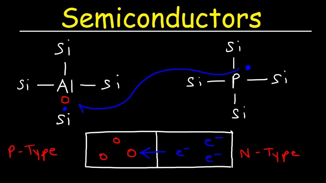
- 😀 A PN Junction Diode is formed by introducing trivalent and pentavalent impurities on a silicon or germanium wafer, resulting in P-type and N-type materials respectively.
- 🔌 The diode consists of two metallic contacts that allow for the application of external voltage across the semiconductor material.
- ⚡ There are three bias conditions for diodes: no bias, forward bias (P-side connected to positive), and reverse bias (P-side connected to negative).
- 📈 The symbol of a PN Junction Diode includes a triangle for the P-side, a vertical line for the N-side, and a representation of the depletion layer.
- 🔄 In forward bias, the current through the diode (I_D) is the majority current minus the reverse saturation current (I_S).
- 🔄 In reverse bias, the only current present is the reverse saturation current (I_S).
- 📊 The diode current (I_D) and voltage (V_D) relation is expressed as I_D = I_S (e^(V_D / (ηV_T)) - 1).
- 🌡️ The thermal voltage (V_T) can be calculated as V_T = T_K / 11600, where T_K is the temperature in Kelvin.
- 📉 The ideality factor (η) ranges between 1 and 2, with different values for germanium and silicon based on operating conditions.
- 🔬 An example calculation for the reverse saturation current (I_S) of a germanium diode shows it to be approximately 0.667 microamperes at room temperature.
Q & A
What is a PN junction diode?
-A PN junction diode, or semiconductor diode, is formed by introducing trivalent impurities (p-type) on one side and pentavalent impurities (n-type) on the other side of a silicon or germanium wafer.
How is p-type material created in a PN junction diode?
-P-type material is created by introducing trivalent impurities into the semiconductor material.
What are the three bias conditions for a PN junction diode?
-The three bias conditions are: no bias (no external voltage), forward bias (p-side connected to positive and n-side to negative), and reverse bias (p-side connected to negative and n-side to positive).
What happens to current flow in forward bias condition?
-In forward bias condition, current flows easily through the diode as the p-side is connected to the positive terminal of the battery, reducing the barrier for charge carriers.
What is the significance of the depletion layer in a PN junction diode?
-The depletion layer acts as a barrier to charge carrier movement. Its width changes with applied voltage, affecting the diode's conductivity.
What is the equation for the diode current-voltage relationship?
-The diode current-voltage relationship is given by the equation I_D = I_S (e^(V_D/(ηV_T)) - 1), where I_D is the diode current, I_S is the reverse saturation current, V_D is the voltage across the diode, η is the ideality factor, and V_T is the thermal voltage.
How is thermal voltage (V_T) calculated?
-Thermal voltage (V_T) is calculated using the formula V_T = T_K / 11600, where T_K is the temperature in Kelvin.
What does the ideality factor (η) represent in the diode equation?
-The ideality factor (η) indicates how closely the diode's behavior follows the ideal diode model, typically having a value of 1 for germanium and 2 for silicon at low current.
What was the example calculation for reverse saturation current (I_S) in the lecture?
-In the example, a germanium diode with a forward voltage of 0.25 volts and a current of 10 mA at room temperature was used to find the reverse saturation current (I_S), which calculated to approximately 0.667 microamperes.
Why is the reverse saturation current considered small?
-The reverse saturation current is considered small because it represents the minimal current that flows in reverse bias conditions, indicating that the diode effectively blocks reverse current except for this leakage.
Outlines

This section is available to paid users only. Please upgrade to access this part.
Upgrade NowMindmap

This section is available to paid users only. Please upgrade to access this part.
Upgrade NowKeywords

This section is available to paid users only. Please upgrade to access this part.
Upgrade NowHighlights

This section is available to paid users only. Please upgrade to access this part.
Upgrade NowTranscripts

This section is available to paid users only. Please upgrade to access this part.
Upgrade NowBrowse More Related Video

Semiconductor PN Junctions, The Depletion Region and Diode Characteristics

Classification of Semiconductors (Intrinsic/Extrinsic, P-Type/N-Type)

Transistors, How do they work?
Semiconductors, Insulators & Conductors, Basic Introduction, N type vs P type Semiconductor

How a DIODE Works?

003 INFORMASI: Pengetahuan Dasar Semikonduktor?
5.0 / 5 (0 votes)