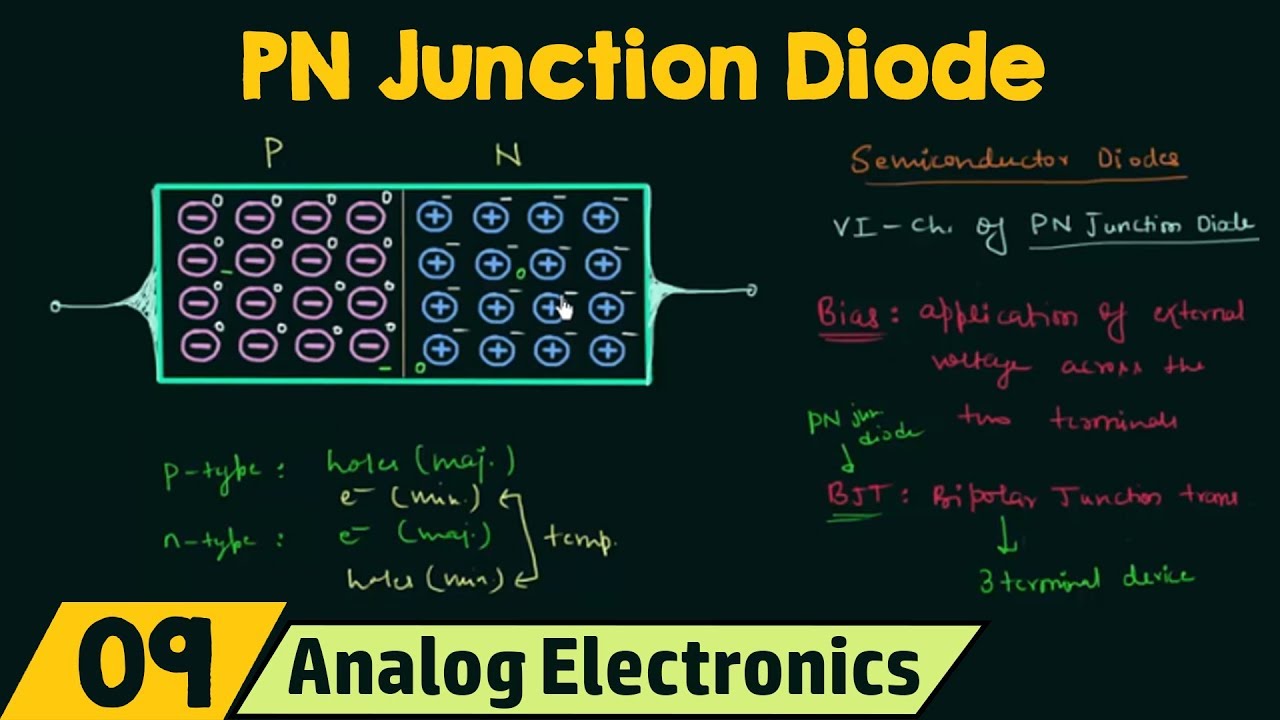
VI Characteristics of PN Junction Diode | PN Junction Forward Bias | PN Junction Reverse Bias
Summary
TLDRThis educational video delves into the voltage-current (V-I) characteristics of PN junction diodes. It explains the formation of ions at the junction of P-type and N-type semiconductors, creating an electric field that impedes current flow. The tutorial covers forward bias, where applying a voltage greater than the potential barrier allows current flow, and reverse bias, where an increased voltage widens the depletion region, preventing current flow except for a minimal leakage from minority carriers. The video concludes with a caution about the potential damage to the diode due to high reverse bias voltages.
Takeaways
- 🔬 When P-type and N-type semiconductor materials are diffused together, a space charge region or depletion region is formed at the junction with positive and negative ions.
- 🔋 The formation of ions at the junction is due to the combination of holes from P-type material and electrons from N-type material, resulting in an electric field that prevents current flow.
- 🔌 In forward bias, the anode should be connected to the positive terminal and the cathode to the negative terminal of the battery, which narrows the depletion region width and allows current to flow.
- 📈 The forward bias characteristic of a PN junction diode shows that current starts to flow when the forward voltage exceeds the threshold voltage, which is approximately 0.7V for silicon and 0.3V for germanium diodes.
- 🔌 In reverse bias, the anode is connected to the negative terminal and the cathode to the positive terminal of the battery, increasing the depletion region width and preventing current flow.
- 📉 The reverse bias characteristic of a PN junction diode shows that current does not flow until a breakdown voltage is reached, after which a large current can flow, potentially damaging the diode.
- 💡 The small current that flows in reverse bias is due to minority charge carriers, which is referred to as reverse saturation current.
- 🚫 If the reverse bias voltage is increased beyond a certain value, the diode may experience a breakdown, leading to a significant increase in current and potential diode damage.
- 📚 Understanding the VI characteristics of a PN junction diode is crucial for comprehending its operation in electronic circuits, including how it behaves under different bias conditions.
Q & A
What happens when P-type and N-type materials are diffused together?
-When P-type and N-type materials are diffused together, a space charge region or depletion region is formed at the junction. This region contains ions, with negative ions on the P-type side and positive ions on the N-type side.
How are ions generated at the junction of P-type and N-type materials?
-Ions are generated at the junction because when P-type material, which has holes, and N-type material, which has electrons, are diffused, the electrons and holes combine. This combination results in the formation of negative ions on the P-type side and positive ions on the N-type side.
What is the role of the electric field formed by the ions in a PN junction?
-The electric field formed by the ions in a PN junction prevents the flow of current until the depletion region is nullified by increasing the forward bias voltage beyond the threshold voltage or potential barrier voltage.
What is the effect of forward bias on the depletion region in a PN junction?
-In forward bias, the depletion region width decreases as the forward voltage increases, allowing current to flow through the PN junction once the voltage exceeds the threshold voltage.
What is the threshold voltage for a silicon diode in forward bias?
-The threshold voltage for a silicon diode in forward bias is 0.7 volts.
What is the threshold voltage for a germanium diode in forward bias?
-The threshold voltage for a germanium diode in forward bias is 0.3 volts.
What happens to the depletion region when a PN junction is reverse biased?
-When a PN junction is reverse biased, the depletion region width increases, preventing the flow of current through the junction.
What is the characteristic of current flow in reverse bias for a PN junction?
-In reverse bias, the current does not flow through the PN junction unless the reverse bias voltage exceeds a certain value leading to breakdown, at which point a large current flows.
What is reverse saturation current and what causes it?
-Reverse saturation current is the small current that flows in reverse bias due to minority charge carriers. It is very minimal and occurs even when the depletion region width increases in reverse bias.
What is the potential risk of applying a reverse bias voltage beyond the breakdown voltage in a PN junction?
-Applying a reverse bias voltage beyond the breakdown voltage can lead to a large current flow, which may damage the PN junction due to the high current.
How can one determine the forward and reverse bias characteristics from the IV curve of a PN junction?
-The forward bias characteristic is in the first quadrant of the IV curve, where current flows after the potential barrier is overcome by the forward voltage. The reverse bias characteristic is in the third quadrant, where current does not flow until breakdown occurs.
Outlines

Cette section est réservée aux utilisateurs payants. Améliorez votre compte pour accéder à cette section.
Améliorer maintenantMindmap

Cette section est réservée aux utilisateurs payants. Améliorez votre compte pour accéder à cette section.
Améliorer maintenantKeywords

Cette section est réservée aux utilisateurs payants. Améliorez votre compte pour accéder à cette section.
Améliorer maintenantHighlights

Cette section est réservée aux utilisateurs payants. Améliorez votre compte pour accéder à cette section.
Améliorer maintenantTranscripts

Cette section est réservée aux utilisateurs payants. Améliorez votre compte pour accéder à cette section.
Améliorer maintenantVoir Plus de Vidéos Connexes

Types of Diodes - The Learning Circuit

Schottky Diode (Construction & Working) Special Purpose Diodes (Basics Electronics)

PN Junction Diode (No Applied Bias)

V-I Characteristics of PN Junction Diode in Hindi | TECH GURUKUL By Dinesh Arya

Semiconductor PN Junctions, The Depletion Region and Diode Characteristics

ohms law class 12 | ohmic and non ohmic devices | limitations of ohms law | 12th class physics
5.0 / 5 (0 votes)
