How a DIODE Works?
Summary
TLDRThis video explains the fundamental concepts of diodes, specifically the PN junction diode. It describes diodes as one-way valves for current flow, introducing semiconductors and their properties. The script details the differences between conductors, insulators, and semiconductors, focusing on silicon and its doping process, which creates p-type and n-type semiconductors. The interaction between these types forms a diode, highlighting the significance of barrier potential and depletion regions. The video also covers forward and reverse biasing, illustrating how current flow is influenced by voltage variations, including the breakdown phenomenon in reverse biasing.
Takeaways
- 😀 Diodes play a crucial role in modern electronics and come in various types, each with unique functions.
- 🔍 A diode acts like a one-way valve, allowing current to flow in one direction while blocking it in the opposite direction.
- ⚛️ Understanding diodes requires a basic knowledge of semiconductors, which are classified as conductors, insulators, and semiconductors based on their conductivity.
- 🔌 Conductors, like copper, have high conductivity, while insulators, like plastic, have low conductivity; semiconductors fall in between.
- 🧪 Silicon and germanium are among the most commonly used semiconductors in electronic applications.
- 💡 Silicon has four valence electrons and forms covalent bonds, making it a poor conductor at normal temperatures.
- 🔬 Doping enhances the conductivity of semiconductors by adding impurities; trivalent impurities create p-type semiconductors, while pentavalent impurities create n-type semiconductors.
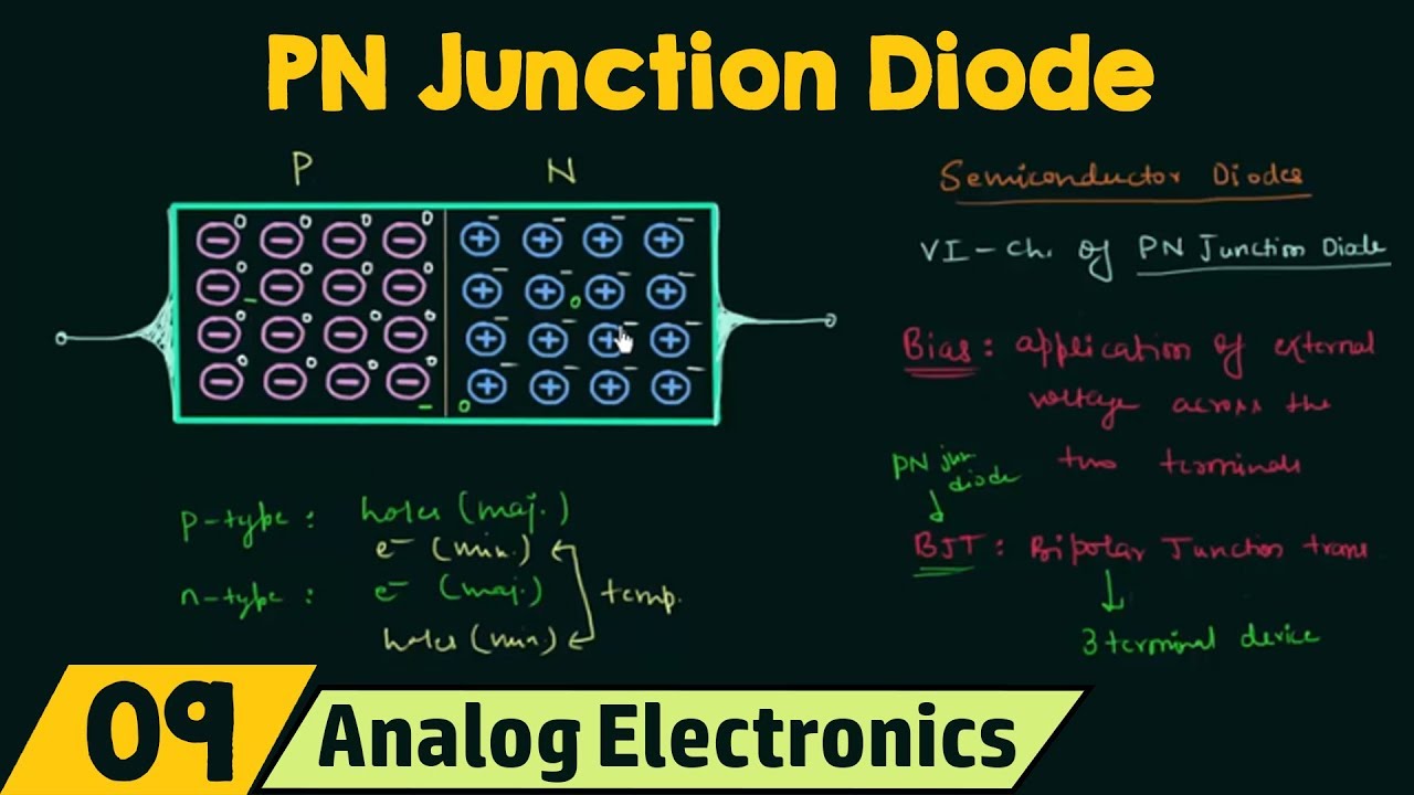
- ⚙️ A PN junction diode is formed by combining p-type and n-type semiconductors, creating a depletion region and a barrier potential.
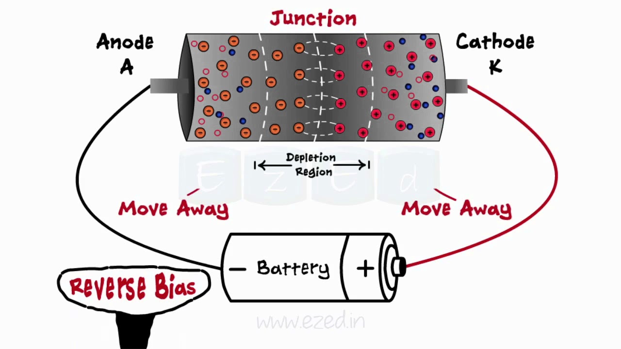
- 🔄 Diodes can be connected in circuits in two ways: forward biasing allows current flow, while reverse biasing blocks it.
- 📈 The VI characteristics of a diode show that it conducts when voltage exceeds the barrier potential and that a breakdown occurs if reverse voltage is increased beyond a certain point.
Q & A
What is a diode and how does it function?
-A diode is a semiconductor device that acts like a one-way valve for electric current, allowing it to flow in one direction while blocking it in the opposite direction.
What are the main types of semiconductors?
-Semiconductors are broadly classified into conductors, insulators, and semiconductors. Common semiconductors include silicon and germanium.
How does silicon behave as a semiconductor?
-Silicon has four valence electrons and forms covalent bonds with neighboring silicon atoms, resulting in no free electrons and making it a poor conductor of electricity at normal temperatures.
What is doping in semiconductors?
-Doping is the process of adding impurities to a pure semiconductor to enhance its conductivity. Impurities can be trivalent (like boron) or pentavalent (like phosphorus).
What are p-type and n-type semiconductors?
-A p-type semiconductor is created when a trivalent impurity is added to pure silicon, resulting in 'holes' (missing electrons). An n-type semiconductor is formed when a pentavalent impurity is added, creating free electrons.
What happens at the atomic level when a PN junction diode is formed?
-In a PN junction diode, free electrons from the n-type region migrate to fill holes in the p-type region, creating a barrier potential that prevents further migration and establishes a depletion region.
What are the two biasing methods for diodes?
-Diodes can be connected in forward biasing or reverse biasing. In forward biasing, the p-side is connected to the positive terminal, allowing current to flow. In reverse biasing, the p-side is connected to the negative terminal, blocking current flow.
What is the barrier potential of a diode?
-The barrier potential is the induced potential created at the junction of p-type and n-type semiconductors, which prevents the further flow of holes and electrons once equilibrium is reached.
What are the VI characteristics of a diode?
-The VI characteristics describe the relationship between voltage and current in a diode. In forward bias, current flows when the applied voltage exceeds the potential barrier. In reverse bias, a constant current flows until breakdown occurs.
What occurs during the breakdown of a diode?
-During breakdown, if the reverse voltage is increased beyond a certain limit, the diode allows a sudden increase in current, which can potentially damage the diode if not controlled.
Outlines

Esta sección está disponible solo para usuarios con suscripción. Por favor, mejora tu plan para acceder a esta parte.
Mejorar ahoraMindmap

Esta sección está disponible solo para usuarios con suscripción. Por favor, mejora tu plan para acceder a esta parte.
Mejorar ahoraKeywords

Esta sección está disponible solo para usuarios con suscripción. Por favor, mejora tu plan para acceder a esta parte.
Mejorar ahoraHighlights

Esta sección está disponible solo para usuarios con suscripción. Por favor, mejora tu plan para acceder a esta parte.
Mejorar ahoraTranscripts

Esta sección está disponible solo para usuarios con suscripción. Por favor, mejora tu plan para acceder a esta parte.
Mejorar ahoraVer Más Videos Relacionados

PN Junction Diode (No Applied Bias)

EL DIODO. CIRCUITOS DE POLARIZACION DIRECTA E INVERSA.

Schottky Diode (Construction & Working) Special Purpose Diodes (Basics Electronics)

Types of Diodes - The Learning Circuit

Diodes - What Are Diodes - PN Junction - Forward Bias - Reverse Bias - Zener Diodes

Diodes Explained - The basics how diodes work working principle pn junction
5.0 / 5 (0 votes)
