VI Characteristics of PN Junction Diode | PN Junction Forward Bias | PN Junction Reverse Bias

Engineering Funda
27 Nov 202309:35

Summary

TLDRThis educational video delves into the voltage-current (V-I) characteristics of PN junction diodes. It explains the formation of ions at the junction of P-type and N-type semiconductors, creating an electric field that impedes current flow. The tutorial covers forward bias, where applying a voltage greater than the potential barrier allows current flow, and reverse bias, where an increased voltage widens the depletion region, preventing current flow except for a minimal leakage from minority carriers. The video concludes with a caution about the potential damage to the diode due to high reverse bias voltages.

Takeaways

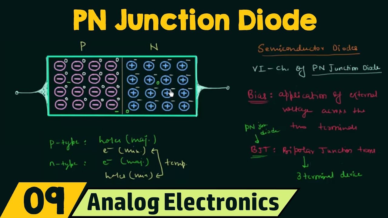
  • 🔬 When P-type and N-type semiconductor materials are diffused together, a space charge region or depletion region is formed at the junction with positive and negative ions.
  • 🔋 The formation of ions at the junction is due to the combination of holes from P-type material and electrons from N-type material, resulting in an electric field that prevents current flow.
  • 🔌 In forward bias, the anode should be connected to the positive terminal and the cathode to the negative terminal of the battery, which narrows the depletion region width and allows current to flow.
  • 📈 The forward bias characteristic of a PN junction diode shows that current starts to flow when the forward voltage exceeds the threshold voltage, which is approximately 0.7V for silicon and 0.3V for germanium diodes.
  • 🔌 In reverse bias, the anode is connected to the negative terminal and the cathode to the positive terminal of the battery, increasing the depletion region width and preventing current flow.
  • 📉 The reverse bias characteristic of a PN junction diode shows that current does not flow until a breakdown voltage is reached, after which a large current can flow, potentially damaging the diode.
  • 💡 The small current that flows in reverse bias is due to minority charge carriers, which is referred to as reverse saturation current.
  • 🚫 If the reverse bias voltage is increased beyond a certain value, the diode may experience a breakdown, leading to a significant increase in current and potential diode damage.
  • 📚 Understanding the VI characteristics of a PN junction diode is crucial for comprehending its operation in electronic circuits, including how it behaves under different bias conditions.

Q & A

  • What happens when P-type and N-type materials are diffused together?

    -When P-type and N-type materials are diffused together, a space charge region or depletion region is formed at the junction. This region contains ions, with negative ions on the P-type side and positive ions on the N-type side.

  • How are ions generated at the junction of P-type and N-type materials?

    -Ions are generated at the junction because when P-type material, which has holes, and N-type material, which has electrons, are diffused, the electrons and holes combine. This combination results in the formation of negative ions on the P-type side and positive ions on the N-type side.

  • What is the role of the electric field formed by the ions in a PN junction?

    -The electric field formed by the ions in a PN junction prevents the flow of current until the depletion region is nullified by increasing the forward bias voltage beyond the threshold voltage or potential barrier voltage.

  • What is the effect of forward bias on the depletion region in a PN junction?

    -In forward bias, the depletion region width decreases as the forward voltage increases, allowing current to flow through the PN junction once the voltage exceeds the threshold voltage.

  • What is the threshold voltage for a silicon diode in forward bias?

    -The threshold voltage for a silicon diode in forward bias is 0.7 volts.

  • What is the threshold voltage for a germanium diode in forward bias?

    -The threshold voltage for a germanium diode in forward bias is 0.3 volts.

  • What happens to the depletion region when a PN junction is reverse biased?

    -When a PN junction is reverse biased, the depletion region width increases, preventing the flow of current through the junction.

  • What is the characteristic of current flow in reverse bias for a PN junction?

    -In reverse bias, the current does not flow through the PN junction unless the reverse bias voltage exceeds a certain value leading to breakdown, at which point a large current flows.

  • What is reverse saturation current and what causes it?

    -Reverse saturation current is the small current that flows in reverse bias due to minority charge carriers. It is very minimal and occurs even when the depletion region width increases in reverse bias.

  • What is the potential risk of applying a reverse bias voltage beyond the breakdown voltage in a PN junction?

    -Applying a reverse bias voltage beyond the breakdown voltage can lead to a large current flow, which may damage the PN junction due to the high current.

  • How can one determine the forward and reverse bias characteristics from the IV curve of a PN junction?

    -The forward bias characteristic is in the first quadrant of the IV curve, where current flows after the potential barrier is overcome by the forward voltage. The reverse bias characteristic is in the third quadrant, where current does not flow until breakdown occurs.

Outlines

00:00

🔬 Understanding PN Junction and Its Formation

This paragraph delves into the fundamentals of PN junction diodes, explaining how they are formed by diffusing P-type and N-type semiconductor materials together. The speaker clarifies that ions are generated at the junction due to the combination of holes from the P-type material and electrons from the N-type material. These ions create an electric field that prevents current flow unless a certain voltage is applied. The explanation sets the stage for understanding the voltage-current (V-I) characteristics of diodes, which is the main focus of the video.

05:01

📈 Exploring the V-I Characteristics of PN Junction Diodes

The second paragraph focuses on the V-I characteristics of PN junction diodes, particularly under forward and reverse bias conditions. In forward bias, the anode is connected to the positive terminal and the cathode to the negative terminal of a battery, narrowing the depletion region and allowing current to flow once the voltage exceeds the threshold or potential barrier voltage. For silicon diodes, this threshold is 0.7 volts, and for germanium, it's 0.3 volts. In reverse bias, the anode is connected to the negative terminal and the cathode to the positive, widening the depletion region and preventing current flow except for a small leakage current due to minority carriers. The speaker warns that exceeding a certain reverse voltage can lead to diode breakdown and significant current flow, which can damage the diode. The paragraph concludes with a brief overview of the forward and reverse bias characteristics, emphasizing the importance of understanding these behaviors for practical applications.

Mindmap

Keywords

💡PN Junction

A PN junction is a boundary or interface between a P-type semiconductor and an N-type semiconductor in a single crystal of semiconductor. It is the fundamental building block of many electronic devices like diodes and transistors. In the video, the PN junction is central to understanding how diodes work, particularly in terms of their voltage-current (V-I) characteristics. The script explains that when P-type and N-type materials are diffused together, a space charge region or depletion region forms at the junction, which is crucial for the diode's operation.

💡Depletion Region

The depletion region is the area in a PN junction where the majority of charge carriers (electrons and holes) have been depleted due to diffusion and recombination. This region contains a high concentration of ionized dopants, creating an electric field that opposes further flow of charge carriers. In the video, the depletion region's width changes with applied voltage, which is a key aspect of the diode's V-I characteristics. The script describes how the depletion region's width narrows under forward bias, allowing current to flow, and widens under reverse bias, preventing current flow.

💡Forward Bias

Forward bias is a condition where the P-type side of a PN junction is connected to the positive terminal of a voltage source, and the N-type side is connected to the negative terminal. This biasing arrangement reduces the potential barrier at the junction, allowing current to flow more easily. The video script explains that in forward bias, the depletion region width decreases with increasing voltage, and current starts to flow once the forward voltage exceeds the potential barrier voltage, which is approximately 0.7 volts for silicon diodes and 0.3 volts for germanium diodes.

💡Reverse Bias

Reverse bias is the opposite of forward bias, where the P-type side of a PN junction is connected to the negative terminal of a voltage source, and the N-type side is connected to the positive terminal. This biasing increases the potential barrier at the junction, making it difficult for current to flow. The video script discusses how, under reverse bias, the depletion region width increases, preventing significant current flow until the reverse voltage reaches a level that causes breakdown, at which point a large current can flow, potentially damaging the diode.

💡Ions

Ions are atoms or molecules that have lost or gained one or more electrons, resulting in a net electric charge. In the context of the video, ions are generated at the PN junction due to the movement of electrons and holes. The script explains that when P-type and N-type materials are diffused together, electrons from the N-type material combine with holes from the P-type material, leaving behind positive and negative ions respectively. These ions contribute to the formation of the depletion region and the electric field that influences the diode's behavior.

💡Space Charge Region

The space charge region, also known as the depletion region, is the area near the PN junction where the free charge carriers are depleted, and the remaining immobile ions create an electric field. This region plays a critical role in the diode's operation by controlling the flow of current. The video script describes how the space charge region's electric field opposes the flow of current and how its width changes with the application of forward or reverse bias.

💡Potential Barrier

The potential barrier is the energy barrier that forms at the PN junction due to the built-in electric field. It acts as a barrier to the flow of majority charge carriers. The video script explains that in forward bias, the potential barrier is reduced, allowing current to flow, while in reverse bias, it is increased, preventing current flow until the reverse voltage is high enough to cause breakdown.

💡Threshold Voltage

Threshold voltage, also known as the knee voltage, is the minimum voltage required to forward bias a PN junction and allow significant current flow. The video script mentions that for silicon diodes, this voltage is typically around 0.7 volts, and for germanium diodes, it is around 0.3 volts. The threshold voltage is a critical parameter in the V-I characteristic curve of a diode, marking the point where the diode starts to conduct.

💡Breakdown Voltage

Breakdown voltage is the voltage at which a significant increase in current occurs due to the diode's structure being compromised, often leading to damage if the current is not limited. In the video script, it is mentioned that if the reverse bias voltage is increased beyond a certain point, the diode can experience breakdown, at which point a large current flows, potentially damaging the diode. This is an important consideration in the design and operation of diodes to ensure they do not exceed their safe operating limits.

💡Minority Carriers

Minority carriers are the charge carriers that are less prevalent in a given type of semiconductor material. In an N-type material, minority carriers are holes, and in a P-type material, they are electrons. The video script explains that under reverse bias, the current that does flow is due to these minority carriers. This current is typically very small and is referred to as the reverse saturation current. The presence of minority carriers is essential for the operation of diodes and transistors, as they facilitate the flow of current under certain conditions.

Highlights

Explanation of PN Junction diode and its VI characteristics.

Formation of ions at the junction of P and N type materials.

Generation of negative ions in P type material and positive ions in N type material.

The role of holes and electrons in the formation of ions at the junction.

Creation of an electric field due to the presence of ions, which prevents current flow.

Description of forward biasing a PN Junction diode.

Narrowing of depletion region width under forward bias.

Requirement of forward voltage to be greater than potential barrier voltage for current flow.

Threshold voltage for silicon diodes is 0.7 volts, and for germanium diodes, it is 0.3 volts.

Current starts to flow in forward bias once the voltage exceeds the threshold.

Explanation of reverse biasing a PN Junction diode.

Increase in depletion region width under reverse bias, preventing current flow.

Minority carrier-induced current flow in reverse bias.

Potential for diode damage due to high current flow post breakdown in reverse bias.

Characteristics of PN Junction diode in forward and reverse bias.

Reverse saturation current due to minority carriers in reverse bias.

Summary of the basic characteristics of PN Junction diodes.

Transcripts

play00:01

Hello friends welcome to engineering

play00:03

Funda family in this video I'll be going

play00:06

to explain you p and Junction diode VI

play00:10

characteristics in my last video I have

play00:13

explained PN Junction diode there are a

play00:16

few basic things that you need to

play00:18

understand before you go for Vi

play00:20

characteristic see when you diffuse P

play00:23

type and end type material together then

play00:25

at

play00:26

Junction there is space charge region or

play00:30

region in this region there are ions see

play00:35

at the side of P type material we have

play00:37

negative ions and at the side of n type

play00:39

material we are having positive ions now

play00:42

question is how these ions are

play00:45

generated see with P type material we

play00:47

don't have ions with n type material we

play00:50

don't have ions but when you diffuse P

play00:52

type and N type material at that time at

play00:55

Junction there is a formation of ions at

play00:59

the side of P type negative ions are

play01:01

generated at the side of n type positive

play01:03

ions are generated but why see when you

play01:07

diffuse materials at that time P type

play01:10

material is having holes n type material

play01:13

is having

play01:14

electrons so electrons and holes are

play01:16

getting combined together so P type

play01:19

material is having holes and that is

play01:23

taking that is consuming electrons and

play01:26

as it consumes electron it is forming

play01:29

negative ions over here and N type

play01:32

material is having electrons it is

play01:34

consuming holes so it is forming

play01:36

positive ions over here right so you'll

play01:39

be observing when you diffuse two

play01:40

materials together at that time there is

play01:43

a formation of ions at the side of P

play01:46

type it consumes electrons means

play01:48

negative charge that's why it forms

play01:51

negative ions and N type material is

play01:53

having electrons it is consuming holes

play01:56

that's why it is forming positive ions

play01:59

holes is is having positive charge

play02:01

that's why it is forming positive ions

play02:04

over here and this ions are resulting

play02:07

into electric field and this electric

play02:10

field will not allow flow of current

play02:13

this electric field will not allow flow

play02:16

of current see this electric field is

play02:18

happening because of depletion region in

play02:21

depletion region we are having positive

play02:23

and negative ions so because of ions

play02:26

there is electric field and that

play02:27

electric field will not allow flow of

play02:30

current right now let me explain how PN

play02:34

Junction VA characteristic is there so

play02:36

in PN Junction see if you want forward

play02:40

bias characteristic then anod should be

play02:43

connected with positive terminal of

play02:45

battery and cathode that should be

play02:48

connected with negative terminal of

play02:50

battery so when you connect anode with

play02:53

positive and cathode with negative you

play02:55

will be connecting this PN Junction in

play02:57

forward bias now in forward bias what

play03:00

happens so in forward bias you'll be

play03:03

observing depletion region width that is

play03:06

getting

play03:07

narrowed so width of depletion region

play03:10

that will decrease as you increase

play03:13

voltage right you see here we are having

play03:16

depletion region without any bias means

play03:19

here we have not connected any Supply

play03:22

now we are connecting that in forward

play03:24

wise for forward wise what we need to do

play03:27

anod with positive and cathode with

play03:29

negative Minal so in this situation

play03:32

depletion region width you see that is

play03:34

decreasing over here so previously

play03:37

depletion region WID that was bit wide

play03:40

but as you increase forward V voltage

play03:41

the depletion region width is decreasing

play03:44

right and this depletion region that

play03:47

doesn't allow flow of current so but

play03:50

obviously for a flow of current for a

play03:52

flow of current this battery is

play03:54

connected so here this battery will be

play03:57

resulting into current in this direction

play03:59

but this current through this PN

play04:01

Junction will not flow until depletion

play04:05

region width so we need to nullify

play04:07

depletion region how by increasing

play04:10

forward W voltage

play04:12

Beyond threshold voltage or you can say

play04:15

forward W voltage should be greater than

play04:17

potential barrier voltage so as you

play04:20

increase as you increase this forward W

play04:22

voltage as you increase this forward wi

play04:25

voltage depletion region width will

play04:26

decrease and if you increase this

play04:28

forward wi voltage Beyond potential

play04:30

barrier then you'll be observing this

play04:33

depletion region that will get nullified

play04:35

after that flow of current will happen

play04:38

in this diode in this Loop right so now

play04:41

let us try to understand characteristic

play04:43

of p and Junction in forward Bas so see

play04:46

initially we are increasing voltage but

play04:49

as depletion region is there flow of

play04:52

current will not

play04:53

happen right but if you increase voltage

play04:58

Beyond threshold volt voltage then

play05:01

current will start to flow so you can

play05:03

observe vertically we have current

play05:05

horizontally we have voltage so if you

play05:07

increase if you

play05:09

increase this voltage Beyond threshold

play05:13

voltage then current will flow right so

play05:16

here see this voltage after which

play05:19

current is Flowing that is theold

play05:21

voltage so that is 0.7 volt in case of

play05:25

silicon diode and that is 0.3

play05:30

in case of germanium diode so that is

play05:33

how simple characteristic is there with

play05:35

PN Junction in forward Bas

play05:38

right up to threshold voltage or up to

play05:41

potential

play05:42

barrier in forward B also current will

play05:45

not flow if you apply voltage greater

play05:48

than potential barrier then current will

play05:51

flow right now let us try to understand

play05:55

reverse bias characteristic so in

play05:57

Reverse bias what we need to do is we

play05:59

need to

play06:00

connect anode with negative terminal of

play06:04

battery and cathode with positive

play06:06

terminal of battery so what will happen

play06:10

as if you connect this PN Junction in

play06:12

Reverse bias the depletion region width

play06:15

will

play06:15

increase it will increase

play06:18

further so what will happen you see as

play06:21

depletion region width is increasing

play06:23

current cannot flow right current in

play06:26

this diode cannot flow see because of

play06:29

battery current should flow like this

play06:31

right current should flow like this but

play06:34

as depletion region with that is getting

play06:37

widen it will not allow flow of current

play06:40

it will not allow flow of current so

play06:42

current cannot flow over here right let

play06:45

me show you in characteristic you see

play06:47

this is voltage and this is what reverse

play06:50

bass so characteristic will come in

play06:53

third quadrant right so in Reverse bias

play06:56

if you increase voltage then you see

play06:59

current will not flow right here current

play07:01

will not flow now you going be thinking

play07:03

like I'm showing you some current right

play07:06

constant current you

play07:07

see so here this

play07:10

current this current that is happening

play07:14

this current that is happening because

play07:15

of minority carrier right so here

play07:19

minority charge carrier allows flow of

play07:22

current but that is very less right and

play07:26

see if you increase this Reverse by

play07:29

voltage

play07:30

Beyond some value then there can be

play07:32

breakdown right so after breakdown after

play07:36

breakdown huge current will flow right

play07:39

after breakdown huge current will flow

play07:41

so if I say this is breakdown

play07:44

voltage right then after breakdown you

play07:48

see huge current will flow and in this

play07:51

situation it is highly possible that P

play07:55

and Junction may get damaged right so

play07:58

here see in Reverse bias current cannnot

play08:02

flow and whatever current current that

play08:04

flows that is due to minority charge

play08:07

carriers only right and here in Reverse

play08:10

B depletion region width that will

play08:12

increase and it will increase based on

play08:15

reverse bias voltage right and after

play08:18

some value there will be breakdown and

play08:20

huge current will flow so here see

play08:23

complete characteristic that I have

play08:26

shown see in forward bias this is

play08:28

forward characteristic in forward West

play08:31

all you need to have is you need to have

play08:35

anod you need to have

play08:38

anode positive with respect to cathode

play08:43

right so characteristic will be in first

play08:45

Quant in which see after potential

play08:49

barrier forward as voltage current will

play08:52

flow and in Reverse bias in Reverse bias

play08:56

anod will be negative right

play09:01

anod will be negative with respect to

play09:05

cathode right so in that case current

play09:09

will not flow right and whatever current

play09:11

that is happening here that is due to

play09:14

minority carrier that one can say that

play09:16

is reverse saturation current right

play09:19

reverse saturation

play09:20

current that is happening because of

play09:23

minority carrier that is how basic

play09:25

characteristic is there with P Junction

play09:27

that I hope you have understood this

play09:29

still if anything that you would like to

play09:30

share please note it down in comment

play09:32

section I'll be happy to help you thank

play09:33

you so much for watching this video

Rate This

5.0 / 5 (0 votes)

相关标签
PN JunctionDiode CharacteristicsElectrical EngineeringSemiconductorsForward BiasReverse BiasPotential BarrierDepletion RegionMinority CarriersBreakdown Voltage
您是否需要英文摘要?