Power Diode Recovered Charge(Qr) & Reverse Recovery Time(trr) || Diode Switching Loss Explanation

Electronics Circuit Hub
20 Oct 201811:32

Summary

TLDRIn this educational lecture, the presenter delves into the concept of stored charge and reverse recovery in diodes. They explain the functioning of a diode under forward and reverse bias, highlighting the role of minority charge carriers and junction capacitance. The lecture further discusses the process of removing stored charges and the significance of reverse recovery time (tRR). It explores power loss in diodes due to stored charges and reverse recovery, and contrasts different types of diodes, such as the IN4007 and SBD, in terms of their reverse recovery characteristics.

Takeaways

  • πŸ”Œ Diodes function by allowing current flow when forward-biased and blocking current when reverse-biased.
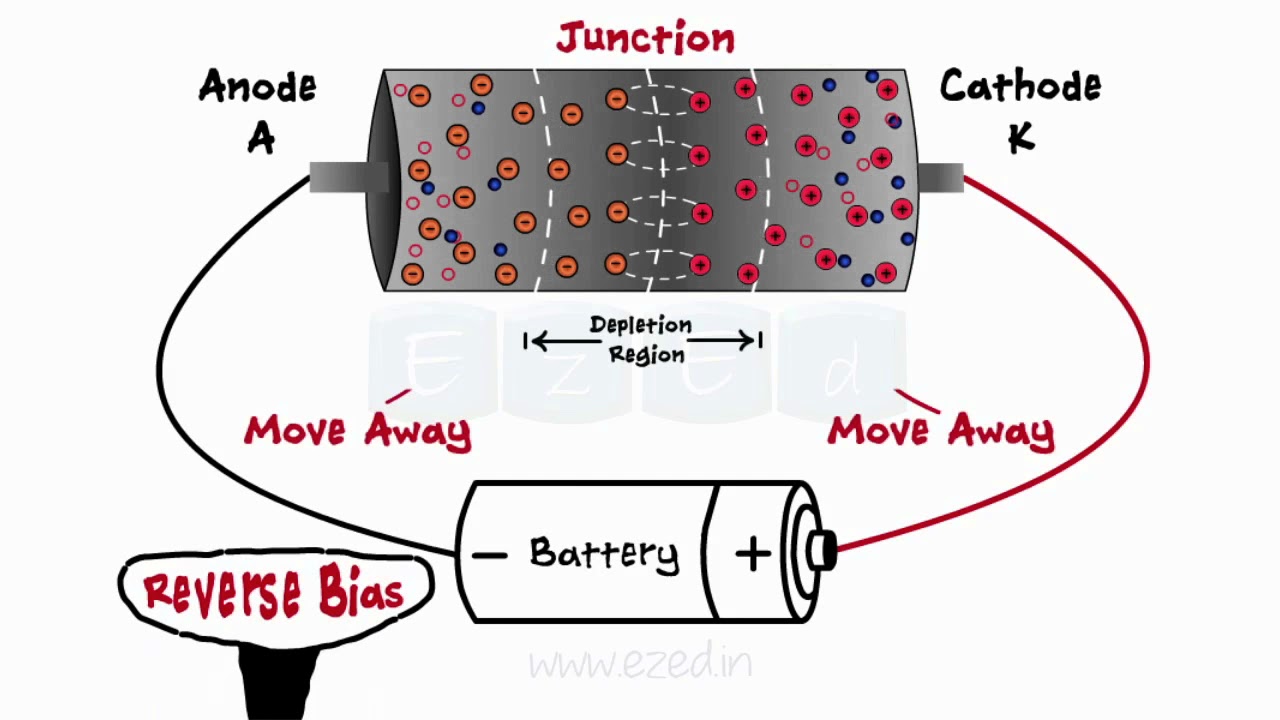
  • 🌊 The depletion region in a diode expands when reverse-biased, which helps to block current flow.
  • ⚑ The process of removing stored charges in a diode's junction capacitance is crucial for its operation.
  • πŸ•’ Reverse recovery time (tRR) is the time it takes for a diode to remove all stored charges and become capable of blocking reverse voltage.
  • πŸ“‰ The waveform of voltage and current across a diode can illustrate the diode's behavior during forward and reverse bias conditions.
  • πŸ”‹ The stored charge in the junction capacitance affects the diode's ability to block reverse voltage, which is significant for its performance.
  • πŸ’‘ The minority charge carriers' diffusion from the P-region to the N-region and vice versa is key to the diode's conduction.
  • πŸ”— The slope of the current during the diode's operation influences the diode's charge and discharge dynamics.
  • πŸ›‘ The removal of stored charges is achieved by applying a reverse voltage, which initiates the reverse recovery process.
  • πŸ“š Different types of diodes, such as Schottky or standard silicon diodes, have varying reverse recovery times and stored charge characteristics.

Q & A

  • What is the main topic of the lecture?

    -The main topic of the lecture is the stored charge and reverse recovery in diodes, including power loss due to stored charges and the concept of reverse recovery time (t_rr) in diodes.

  • What happens when a diode is forward biased?

    -When a diode is forward biased, the depletion region reduces, allowing current to flow through it due to the diffusion of minority charge carriers from the P region to the N region and vice versa.

  • How does the depletion region change when a diode is reverse biased?

    -When a diode is reverse biased, the depletion region spreads towards the PN junction, and the minority carrier charges are pulled out, preventing current flow until the diode is capable of blocking the reverse voltage.

  • What is meant by stored charge in a diode?

    -Stored charge in a diode refers to the minority charge carriers that accumulate at the junction capacitance when the diode is forward biased.

  • What is reverse recovery?

    -Reverse recovery is the process of removing the stored charges from the junction capacitance when the diode transitions from forward bias to reverse bias.

  • How is the reverse recovery time (t_rr) defined?

    -The reverse recovery time (t_rr) is the time required for a diode to remove all stored charges and block the applied reverse voltage after transitioning from forward bias to reverse bias.

  • What is the significance of the current slope during reverse recovery?

    -The current slope during reverse recovery is significant as it determines the rate at which the stored charges are removed and the diode's ability to block the reverse voltage.

  • What are the power losses in a diode during reverse recovery?

    -Power losses in a diode during reverse recovery include conduction losses when the diode is forward biased and switching losses when the diode transitions to reverse bias.

  • Why is it important to know the reverse recovery time for diodes?

    -Knowing the reverse recovery time is important because it affects the efficiency and performance of circuits, especially in applications involving fast switching.

  • How do different types of diodes compare in terms of reverse recovery time?

    -Different types of diodes have different reverse recovery times. For example, Schottky diodes typically have faster reverse recovery times compared to silicon diodes, which is an important consideration in high-speed switching applications.

Outlines

00:00

πŸ”¬ Introduction to Stored Charge and Diode Operations

This paragraph introduces the topic of stored charge and diode behavior, particularly focusing on reverse recovery and power loss due to stored charges. The speaker begins by inviting viewers to subscribe to the channel and engage with the content. The main discussion revolves around the functioning of a diode, explaining how a forward bias leads to the diffusion of minority charge carriers and the resulting current flow. The concept of junction capacitance charging and the role of the depletion region in a PN junction diode are also covered. The paragraph sets the stage for a deeper dive into the technical aspects of diode operation and the challenges associated with stored charges and reverse recovery.

05:03

πŸ”‹ Reverse Bias and Diode Recovery Process

The second paragraph delves into the process of reverse biasing a diode and the subsequent removal of stored charges. It describes how applying a reverse voltage leads to the depletion of minority charge carriers and the expansion of the depletion region. The speaker uses a waveform diagram to illustrate the voltage and current changes over time, highlighting the intervals during which the diode transitions from forward to reverse bias. The concept of reverse recovery time (tRR) is introduced, explaining the time it takes for a diode to remove all stored charges and become capable of blocking reverse voltage. The paragraph also touches on the impact of the slope of the current on the diode's behavior, providing a technical explanation of the recovery process.

10:07

⏱ Understanding Reverse Recovery Time and Diode Types

The final paragraph discusses the reverse recovery time (TRR) in detail, emphasizing its significance in determining the diode's ability to block negative voltage after charge removal. The speaker contrasts different types of diodes, such as the IN4001 and Schottky diodes, highlighting their respective TRR characteristics. The paragraph concludes with a summary of the lecture's key points and a thank you to the viewers for their attention. It reinforces the importance of understanding the technical specifications of diodes for applications involving rapid switching and voltage blocking.

Mindmap

Keywords

πŸ’‘Stored Charge

Stored charge refers to the accumulation of charge carriers within the junction capacitance of a diode. In the context of the video, when a diode is forward-biased, minority charge carriers diffuse across the PN junction, leading to the storage of these charges. This stored charge plays a crucial role in the diode's operation and its ability to conduct current. The video discusses the process of removing these stored charges during reverse recovery, which is essential for the diode's proper functioning.

πŸ’‘Diode

A diode is a two-terminal electronic component that allows current to flow primarily in one direction. It consists of a PN junction, which is a boundary between a P-type semiconductor and an N-type semiconductor. The video focuses on the behavior of diodes under different biasing conditions, such as forward and reverse bias, and the impact of stored charges on their performance.

πŸ’‘Reverse Recovery

Reverse recovery is the process of removing stored charges from the junction capacitance of a diode when it transitions from forward bias to reverse bias. This process is critical for the diode's ability to block reverse voltage and is characterized by the reverse recovery time (tRR). The video explains that during reverse recovery, a negative current is used to extract minority carriers, which is illustrated through the waveforms and charge distribution diagrams presented.

πŸ’‘Power Loss

Power loss in a diode refers to the energy dissipated as heat when current flows through the diode, particularly during the switching process. The video discusses two types of losses: conduction loss, which occurs when the diode is forward-biased and current flows, and switching loss, which happens during the transition from forward to reverse bias. Understanding power loss is important for designing efficient electronic circuits.

πŸ’‘tRR (Reverse Recovery Time)

tRR, or reverse recovery time, is the time it takes for a diode to remove all stored charges and become capable of blocking reverse voltage after being switched off. This parameter is crucial for high-speed switching applications where rapid diode recovery is necessary. The video mentions that different types of diodes have different tRR values, which can affect their performance in specific applications.

πŸ’‘QR (Recovery Charge)

QR, or recovery charge, is the amount of charge that must be removed from the diode's junction capacitance during reverse recovery. It is represented by the area under the current waveform during the reverse recovery period. The video uses QR as an example to illustrate the relationship between the stored charge and the diode's reverse recovery characteristics.

πŸ’‘PN Junction

The PN junction is the interface between P-type and N-type semiconductor materials in a diode. It is the fundamental structure that allows the diode to exhibit its unidirectional conductivity. The video explains how the depletion region of the PN junction changes with forward and reverse bias, affecting the diode's behavior and the storage of charge carriers.

πŸ’‘Depletion Region

The depletion region is the area near the PN junction where the majority of charge carriers have been depleted, leaving behind an electric field that opposes further flow of current. The video describes how the width of the depletion region changes with biasing conditions, affecting the diode's ability to conduct or block current.

πŸ’‘Forward Bias

Forward bias is a condition where a diode is connected in such a way that its P-type side is connected to the positive terminal of a voltage source, and its N-type side is connected to the negative terminal. This biasing condition allows current to flow easily through the diode. The video discusses how forward bias leads to the diffusion of minority charge carriers and the storage of charge in the junction capacitance.

πŸ’‘Reverse Bias

Reverse bias is the opposite of forward bias, where the P-type side of a diode is connected to the negative terminal of a voltage source, and the N-type side is connected to the positive terminal. This biasing condition causes the depletion region to widen, making it difficult for current to flow. The video explains the process of removing stored charges when a diode transitions from forward to reverse bias.

πŸ’‘Diode Types

The video mentions different types of diodes, such as the IN4007 and SBD (Schottky Barrier Diode), and discusses their specific reverse recovery characteristics. Different diode types have different materials and structures, which affect their performance parameters like reverse recovery time and stored charge. Understanding these differences is important for selecting the appropriate diode for a given application.

Highlights

Introduction to stored charge and diode reverse recovery

Explanation of power loss in diodes due to stored charges and reverse recovery

Definition of tRR (reverse recovery time) and QR (reverse recovery charge)

Types of diodes and their reverse recovery times

How to subscribe and receive notifications for upcoming lectures

Basic functioning of a diode under forward bias

The role of minority charge carriers in diode operation

How the depletion region changes under reverse bias

Process of removing stored charges in the junction capacitance

Waveform analysis of voltage and current across a diode

Minority charge distribution during reverse recovery

Interval analysis of diode operation from on to off state

Impact of current slope on diode performance

Explanation of how depletion region width increases after removing stored charges

Blocking of reverse voltage by diodes after charge removal

Calculation of power loss in diodes during conduction and switching

Detailed discussion on reverse recovery time (TRR) and its significance

Comparison of reverse recovery times for different types of diodes

Conclusion and appreciation for watching the lecture

Transcripts

play00:01

hello friends hope you are doing well in

play00:05

today's lecture I'm going to talk about

play00:09

the stored charge and diode and diode

play00:13

reverse recovery okay power loss in

play00:17

diode due to store charts and reverse

play00:20

recovery and then what is t RR win diode

play00:24

what is QR n diode types of diode and

play00:29

their reverse recovery time so okay so

play00:35

before I start my lecture I would

play00:38

request you if you haven't subscribe my

play00:40

channel please subscribe it and press

play00:45

the bell icon so that you get

play00:48

notifications of all my upcoming lecture

play00:51

please like share with your friends and

play00:55

family members okay watch the video till

play01:00

the end so that you get all the lecture

play01:05

notes ok now let's talk about the diode

play01:12

store charts removal and reverse

play01:15

recovery ok

play01:17

I'm not going much more in detail how

play01:20

diode is functioning but let's talk

play01:23

about a bit a little bit how the hood is

play01:27

working now so if you apply a positive

play01:31

voltage to P reason and negative voltage

play01:36

to n reason okay so what happens is if

play01:42

you apply positive voltage to P reason

play01:45

and negative voltage to n vision there

play01:47

is a magnetic diffusion of a minority

play01:50

carry a charge carrier minority charge

play01:54

carrier from P reason to and reason and

play01:57

indecent to P reason okay

play02:02

minority it's the charge carrier

play02:04

diffuses from P reason to and isn't due

play02:08

to that the junction

play02:11

capacitance charges and because of that

play02:14

the current start flowing through the

play02:17

through it okay so if you apply a

play02:20

forward bias diode in a foul road for

play02:24

advice

play02:25

okay so depletion region of PN Junction

play02:29

diode a diode reduces because of that

play02:33

current start flowing through it okay

play02:36

okay all right so if you bias a diode in

play02:41

a reverse fashion okay how would you

play02:44

guys it if you apply negative voltage to

play02:48

be terminal of PN Junction and positive

play02:53

voltage to end a zone of PN Junction

play02:56

diode becomes a reverse biased reverse

play02:59

bias condition in that particular

play03:01

condition the depletion region spreads

play03:07

towards towards PN and reason and the

play03:12

minority carrier charges now pulls out

play03:15

okay

play03:16

so that is how a diode is working so now

play03:20

let's talk about the store charts in

play03:23

removal and reverse recovery means how

play03:26

you how you remove the stored charges in

play03:30

junction capacitance and what is reverse

play03:33

recovery

play03:33

okay let's talk a bit about that so now

play03:40

okay

play03:42

I have drawn a drawn a waveform this is

play03:49

VD voltage across diode okay over a

play03:52

period of time this is ID current across

play03:56

the diode over a period of time okay and

play03:59

this one I have drawn here minority

play04:03

charge distribution during reverse

play04:05

recovery in diode okay so let's talk

play04:09

about now okay during interval or during

play04:19

interval T equals to zero here

play04:22

to t equals to t0 here okay during

play04:26

interval T equals to 0 to T equals to t0

play04:29

diode is on condition and there is some

play04:33

current current flowing through it okay

play04:35

so that is ID

play04:38

okay so diode is there is some voltage

play04:41

across the diode and some current

play04:43

flowing through it so voltage across

play04:44

diode is VD on and some current across

play04:48

the diode is flowing through it is ID on

play04:51

right okay means diode is in forward

play04:54

bias condition now

play04:59

during interval t equals 2t 0 to t

play05:02

equals to t1 okay t equals 2t 0 to t

play05:07

equals to t1 you have applied the

play05:11

reverse voltage across the PN Junction

play05:13

and diode is in reverse bias condition

play05:16

so now in diode is in reverse bias

play05:20

condition so what happens when the diode

play05:24

is in reverse bias condition means we

play05:27

start removing minority charges with a

play05:30

negative current okay okay so we start

play05:35

removing negative charges from negative

play05:39

current so you can see here there is

play05:43

some negative current flowing through

play05:44

the diode okay now what happens during

play05:51

interval of T equals 2 T 1 2 T equals 2

play05:54

T 2 okay during this interval T equals 2

play05:57

T 1 2 T equals 2 T 2 okay in this

play06:02

interval a diode is off and if we

play06:06

removed the enough charge okay and that

play06:10

point of time voltage across depletion

play06:13

region start decreasing and go negative

play06:19

okay at that point of time voltage

play06:25

across depletion region okay start

play06:29

decreasing and go negative

play06:34

okay during t equals to this point of

play06:37

time okay now let's have a look off

play06:41

minority charge distribution how it is

play06:44

functioning when diode is in forward

play06:47

bias let's say T equals 2t 0 time

play06:50

Junction capacitance fully charged okay

play06:54

there is chards concept a concentration

play06:56

profile over here the junction minority

play06:59

charges are minority charge carriers

play07:03

stored in a junction capacitance over T

play07:06

equals to zero

play07:08

during the period of T equals 2t one

play07:11

start removing some charges from you

play07:14

start pulling out some charges from the

play07:17

from Junction capacitance okay over P

play07:20

and n region so now here the now here

play07:26

you have less charge stored in in the

play07:31

junction capacitance okay all right

play07:34

nothing one more thing

play07:37

the there is a some current slope okay

play07:41

okay this is some slope current slope

play07:45

right that the slope determines the

play07:47

diffusion did and charge and the current

play07:50

okay so at the point of 2 T 2 you have

play07:56

reduced some more charges you have

play08:00

reduced enough charges you have reduced

play08:03

enough charges and that point of time

play08:05

voltage across depletion region start

play08:08

decreasing and go negative so okay

play08:11

during two teeth okay during this period

play08:16

t three okay during this period t three

play08:21

you removed all stored charge in

play08:24

Junction capacitance right so let's say

play08:27

here here okay let's say here let's say

play08:32

here earlier your depletion width reason

play08:36

width is that much only okay that much

play08:39

only now once you removed all charge

play08:42

stored in Junction capacitance okay so

play08:45

your depletion region

play08:48

width increases earlier it was that much

play08:52

now it was that much because you removed

play08:55

all stool charts from the new Junction

play08:57

capacitance so you remove all minority

play09:01

carrier charges from your Junction

play09:03

capacitance so the depletion region

play09:05

width increases because of that diode is

play09:09

now able to block the reverse voltage

play09:12

okay

play09:13

okay diode is now able to block the

play09:17

reverse voltage okay here beauty of -

play09:21

negative voltage okay and there is no

play09:24

current flowing through it so alright

play09:27

hope you understood that much and now

play09:30

let's talk about much more and this

play09:33

interval I've already explained during

play09:37

this now let's talk about loss in power

play09:40

loss in diode what is power loss P

play09:42

equals to B into y at time T equals 2 T

play09:46

0 - 2 equals 2t to zero here it is so

play09:52

nice conduction loss at T equals to G T

play09:55

0 and T equals to t4 you have switching

play09:59

losses right so now what is a reverse

play10:06

recovery time time required to diode to

play10:11

remove all Stuart charts and block the

play10:14

apply negative voltage okay this one is

play10:19

TR from T equals to 0 to P equals to 2

play10:22

for that much time required diode to

play10:25

remove all its two charges that time is

play10:29

called reverse recovery time now what is

play10:31

recovered charge negative diode current

play10:35

area during reverse recovery let's say I

play10:38

will overlook here diode stored charge

play10:42

okay so this one is a recovered charges

play10:46

area okay let's example I n400 say one

play10:51

the TR are not specified then FASTA

play10:54

comedy diode the example is I n for one

play10:59

for it it's TR r equals two now

play11:01

a Schottky diode let's say SB 180 and no

play11:07

recovered charts okay so my question is

play11:10

now while does I even four zero zero

play11:15

seven and SB 1 at T does not have it TRR

play11:18

the reverse recovery time okay okay

play11:21

thank you watching this lecture hope you

play11:24

enjoyed the lecture I wish you a very

play11:27

happy learning

play11:28

thank you so much

Rate This
β˜…
β˜…
β˜…
β˜…
β˜…

5.0 / 5 (0 votes)

Related Tags
Diode BasicsStored ChargeReverse RecoveryPN JunctionElectrical EngineeringSemiconductorsPower LossLecture SeriesEducational ContentTechnical Tutorial