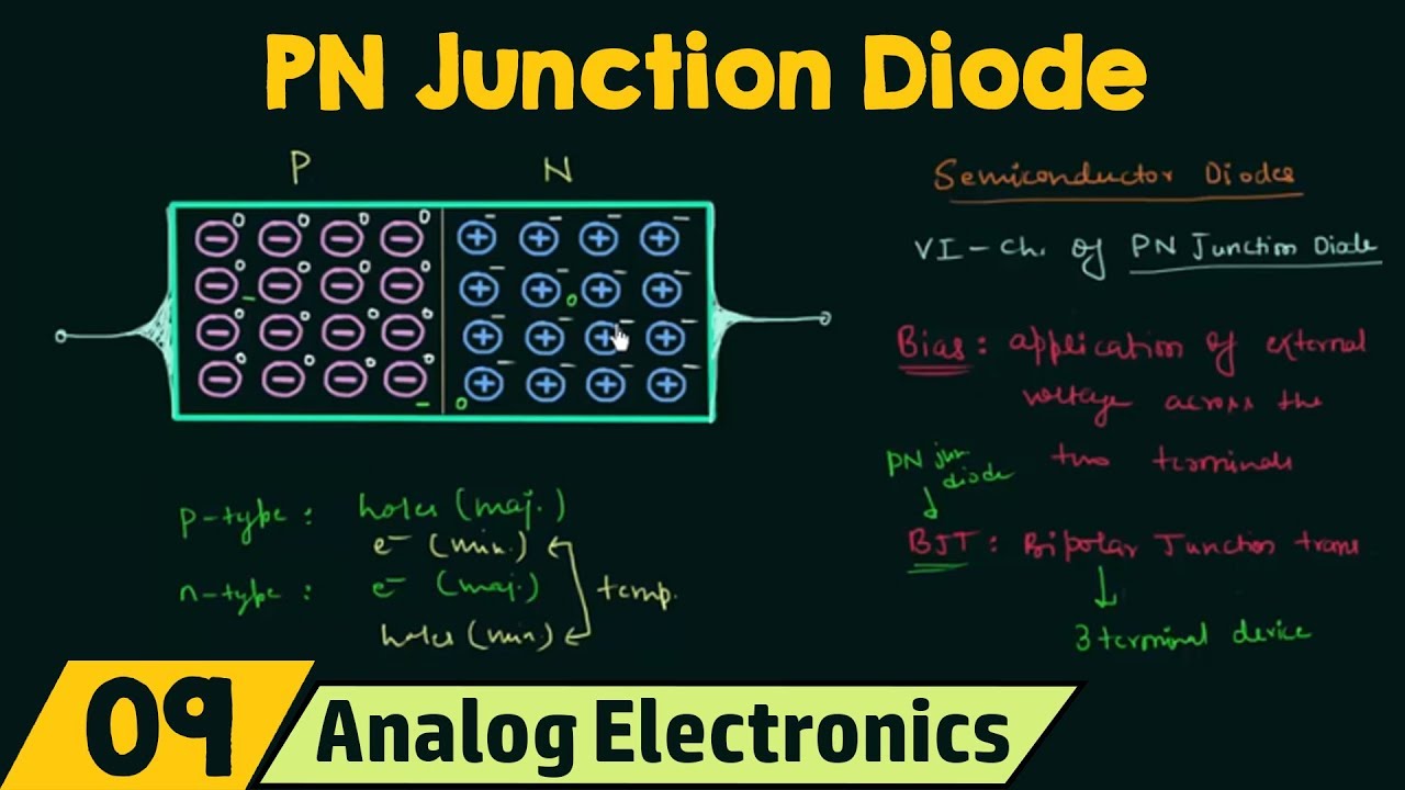
5.1 Forward and reverse biased PN junctions

NPTEL-NOC IITM
11 Oct 202225:01

Summary

TLDRThis lecture delves into the behavior of PN junctions under external bias, contrasting forward and reverse biases. It explains how forward bias reduces the barrier for carrier diffusion, allowing current flow, while reverse bias increases the barrier, halting diffusion and emphasizing drift current. The lecture also introduces the concept of energy band diagrams, illustrating how applied voltage shifts Fermi levels and alters the depletion region's width. The instructor emphasizes the importance of understanding these principles for grasping semiconductor device operation, with a promise to explore quantitative aspects and minority carrier behavior in upcoming sessions.

Takeaways

  • ๐Ÿ”ฌ The lecture discusses the behavior of PN junctions under different bias conditions, focusing on the changes in the depletion layer and electric field.
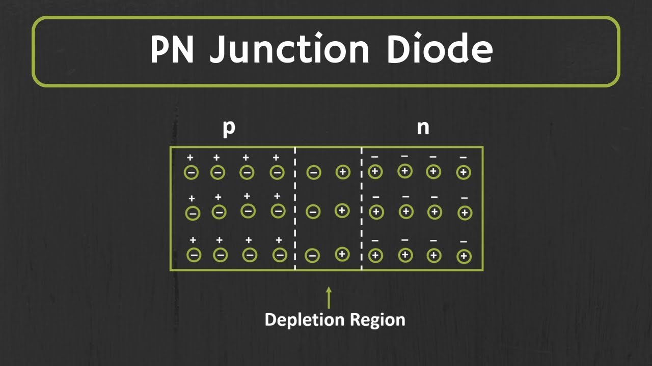
  • ๐Ÿ”‹ When no external voltage is applied, the PN junction is in equilibrium with a uniform Fermi level across it, and there is no current flow due to the potential barrier.
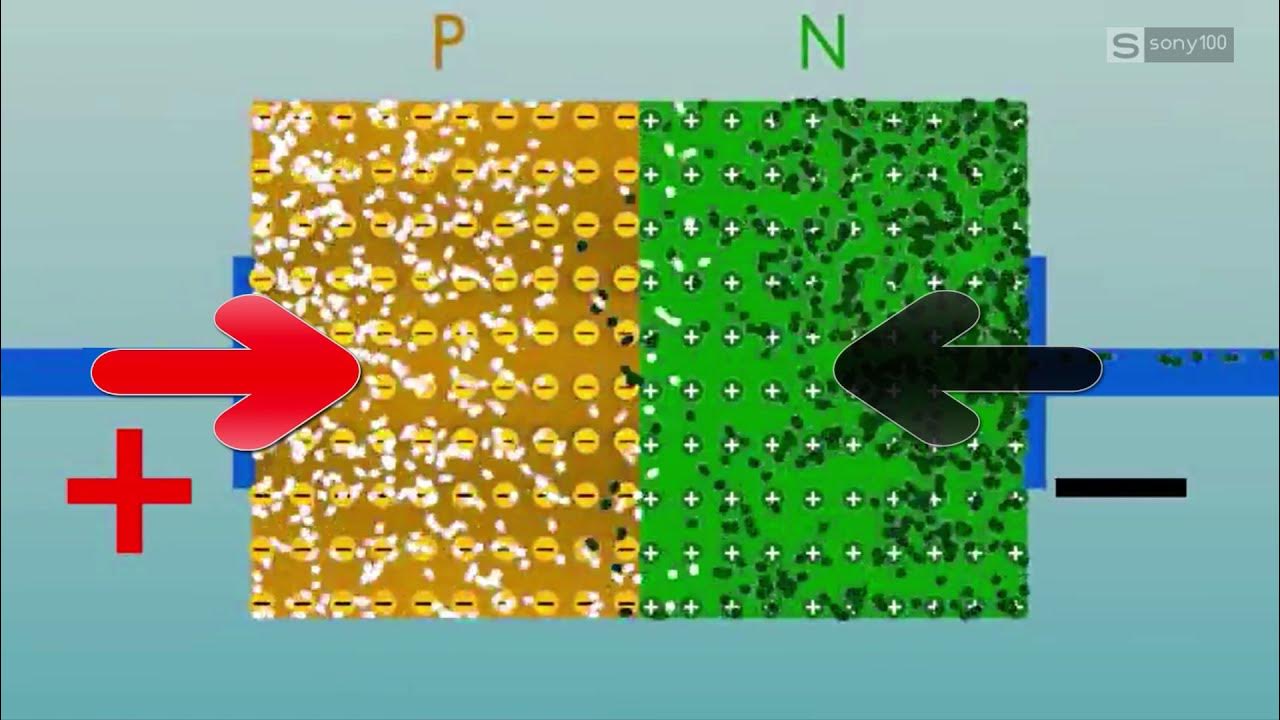
  • โšก In forward bias, a positive voltage is applied to the P-type semiconductor, which reduces the potential barrier and allows majority carriers to diffuse into the depletion region, leading to a decrease in space charge density and depletion width.
  • ๐Ÿ”Œ Under reverse bias, a negative voltage is applied to the P-type semiconductor, increasing the potential barrier and causing majority carriers to move out of the PN junction, increasing the space charge density and depletion width.
  • ๐Ÿ“‰ The energy band diagram of a PN junction changes with the application of voltage, with the Fermi level shifting down in forward bias and up in reverse bias.
  • ๐Ÿ”‘ The lecture emphasizes the importance of understanding the energy band diagrams to grasp the fundamental physics of how PN junctions operate.
  • ๐Ÿšซ In forward bias, the diffusion of majority carriers is dominant, and the drift current of minority carriers can be considered negligible.
  • ๐Ÿ“ˆ In reverse bias, the drift current becomes significant because the increased potential barrier prevents significant carrier diffusion.
  • ๐Ÿ“š The lecture provides a recipe for drawing energy band diagrams under different biases, which is crucial for understanding the behavior of PN junctions.
  • ๐Ÿ”ฎ Upcoming lectures will delve into the quantitative aspects of PN junctions, including the analysis of minority carrier distributions and their impact on current flow.

Q & A

  • What is a PN junction and what happens when an external bias is applied?

    -A PN junction is a semiconductor device formed by joining P-type and N-type semiconductors. When an external bias is applied, it affects the potential barrier, allowing for the movement of majority carriers into the depletion region under forward bias, or out of the junction under reverse bias.

  • How does the depletion layer change when a forward bias is applied to a PN junction?

    -Under forward bias, the depletion layer width decreases because the external voltage reduces the potential barrier, allowing majority carriers to diffuse into the depletion region, leading to a reduction in space charge density.

  • What is the effect of reverse bias on the depletion region of a PN junction?

    -Reverse bias increases the depletion region width and the potential barrier. This causes majority carriers to move out of the PN junction, increasing the space charge density and leaving behind uncompensated ionized dopants.

  • What is the built-in potential (qVbi) and how does it relate to the Fermi level?

    -The built-in potential (qVbi) represents the potential barrier at the PN junction when no external bias is applied. It is related to the Fermi level, which is uniform across the junction in equilibrium, and is defined as the built-in voltage times the charge, giving the potential barrier in electron volts.

  • Why is there no current flow in a PN junction without an external voltage?

    -Without an external voltage, the potential barrier prevents the diffusion of majority carriers across the junction. Electrons cannot move from the N-type to the P-type, and holes cannot move from the P-type to the N-type, resulting in no current flow.

  • How does the Fermi level shift when a positive voltage is applied to a semiconductor?

    -When a positive voltage is applied to a semiconductor, the Fermi level shifts lower because it is analogous to removing electrons from the semiconductor, similar to lowering the water level in a tank.

  • What is the significance of the energy band diagram in understanding the operation of a PN junction?

    -The energy band diagram is crucial for visualizing the changes in the semiconductor's energy levels under different biases. It helps to understand how the applied voltage alters the potential barrier, allowing or preventing the diffusion of carriers.

  • What are the two types of current in semiconductors and how do they relate to the operation of a PN junction?

    -The two types of current in semiconductors are diffusion current, which occurs due to a gradient in carrier concentration, and drift current, which is caused by an electric field. In a PN junction, diffusion current is significant in forward bias, while drift current becomes important in reverse bias.

  • Why can the drift current of minority carriers be neglected in forward bias but not in reverse bias?

    -In forward bias, the majority carrier diffusion is dominant due to the reduced potential barrier, making the drift current of minority carriers negligible. In reverse bias, the potential barrier is increased, preventing majority carrier diffusion, thus making the drift current of minority carriers significant.

  • What will be discussed in the next video regarding the quantitative aspects of PN junctions?

    -The next video will delve into the quantitative aspects of PN junctions, including the study of how minority carrier distribution changes under different biases and the derivation of expressions for these distributions.

Outlines

00:00

๐Ÿ”ฌ Introduction to PN Junctions and External Bias

This paragraph introduces the topic of PN junctions in semiconductor devices, building upon the basic concepts discussed in previous sessions. It focuses on the behavior of PN junctions under the influence of an external bias. The instructor explains the concept of the depletion layer, electric field, and built-in potential in a PN junction without bias. The discussion then shifts to the effects of applying an external voltage, either forward or reverse, and how it alters the equilibrium of the PN junction. The instructor uses a battery model to illustrate the connection and the resulting changes in the Fermi level and potential barrier.

05:06

๐Ÿ”‹ Impact of Reverse Bias on PN Junctions

In this segment, the video script delves into the specifics of what occurs when a reverse bias is applied to a PN junction. The instructor explains that under reverse bias, majority carriers are drawn out of the junction, leading to an increase in the depletion region's width and space charge density. This is due to the additional voltage aiding in the removal of majority carriers, thus disrupting the equilibrium. The discussion serves as a fundamental principle in understanding the operation of PN junctions, with the instructor emphasizing the importance of visualizing these concepts through energy band diagrams.

10:08

๐Ÿ“š Energy Band Diagrams and Applied Voltage

The focus of this paragraph is on the energy band diagrams of PN junctions under different voltage conditions. The instructor provides a step-by-step guide on how to draw these diagrams, starting with the Fermi level and then moving on to the conduction and valence bands for both P and N type semiconductors. The explanation includes how applying a positive or negative voltage affects the position of the Fermi level and, consequently, the energy barrier for carrier movement. The paragraph concludes with a practical recipe for drawing accurate band diagrams, which is crucial for understanding the physics behind semiconductor devices.

15:13

๐Ÿš€ Forward Bias and Carrier Diffusion

This paragraph explores the effects of forward bias on PN junctions, highlighting how the applied voltage reduces the energy barrier, allowing for carrier diffusion. The instructor explains that under forward bias, electrons from the N-type semiconductor and holes from the P-type semiconductor can diffuse across the junction due to the lowered barrier. The discussion also touches on the direction of current flow and the distinction between diffusion and drift currents. It is noted that while drift current exists, it is negligible compared to the diffusion current in forward bias, making the latter the dominant factor in current flow.

20:15

๐Ÿ”„ Reverse Bias and Drift Current

The final paragraph of the script addresses the scenario under reverse bias, where the energy barrier is increased, preventing carrier diffusion. The instructor points out that the dominant current flow in this case is the drift current, which is significant due to the increased barrier height. The discussion serves as a transition to the next video, where the focus will be on quantitative aspects and the behavior of minority carriers. The instructor emphasizes the importance of understanding how minority carrier distributions change under different biases and their impact on current flow, setting the stage for a deeper dive into the physics of PN junctions.

Mindmap

Keywords

๐Ÿ’กPN junction

A PN junction is a boundary or interface between a P-type semiconductor and an N-type semiconductor in a single crystal of semiconductor. It is a fundamental building block in semiconductor devices. In the video, the concept of the PN junction is central to understanding how semiconductor devices function. The script discusses how the depletion layer and electric field within the junction behave under different biases, which is crucial for the operation of diodes and transistors.

๐Ÿ’กDepletion layer

The depletion layer is the region in a PN junction that is devoid of free charge carriers (electrons and holes). It forms due to the diffusion of electrons from the N-type region and holes from the P-type region, leaving behind ionized donor and acceptor impurities. The script explains that the depletion layer plays a critical role in determining the electrical properties of the PN junction, particularly the electric field and potential barrier that influence current flow.

๐Ÿ’กElectric field

In the context of the video, the electric field refers to the field that exists within the depletion region of a PN junction. This field is established due to the separation of charges within the depletion layer and opposes the diffusion of majority carriers. The script describes how the electric field changes when an external bias is applied, which in turn affects the current flow across the junction.

๐Ÿ’กBuilt-in potential

The built-in potential, also known as the intrinsic potential, is the potential difference that exists across a PN junction when no external voltage is applied. It arises due to the alignment of the Fermi levels of the P and N materials. The script mentions that this potential is crucial for understanding the equilibrium state of the PN junction and how it influences the movement of charge carriers.

๐Ÿ’กExternal bias

External bias refers to the voltage applied to a PN junction from an external source, such as a battery. The script discusses two types of external biases: forward bias and reverse bias. These biases significantly affect the behavior of the PN junction, altering the potential barrier and thus the flow of current. Understanding external bias is essential for controlling the operation of semiconductor devices.

๐Ÿ’กForward bias

Forward bias is a condition where the external voltage applied to a PN junction is in the direction that lowers the potential barrier. In the script, it is explained that under forward bias, majority carriers from both P and N sides are driven into the depletion region, reducing the barrier and allowing current to flow more easily. This concept is key to understanding how diodes conduct in the forward direction.

๐Ÿ’กReverse bias

Reverse bias is the opposite of forward bias, where the external voltage increases the potential barrier at the PN junction. The script describes how, under reverse bias, majority carriers are swept out of the junction, increasing the barrier and thus impeding the flow of current. This principle is fundamental to the blocking behavior of diodes when reverse-biased.

๐Ÿ’กFermi level

The Fermi level, or Fermi energy, is the energy level at which the probability of finding an electron in a material is half. In the script, the Fermi level is discussed in the context of how it aligns and shifts in response to applied voltages, influencing the distribution of electrons and holes in the semiconductor. The uniformity or shift of the Fermi level is indicative of the equilibrium or bias conditions of the PN junction.

๐Ÿ’กDoping

Doping is the intentional introduction of impurities into a semiconductor to modify its electrical properties. The script mentions P-type and N-type semiconductors, which are created by doping with acceptor and donor impurities, respectively. Doping establishes the majority charge carriers (holes in P-type, electrons in N-type) and is essential for creating the necessary conditions for a PN junction to function.

๐Ÿ’กEnergy band diagram

An energy band diagram is a graphical representation of the energy levels of electrons in a material. In the script, energy band diagrams are used to illustrate the changes in the semiconductor's energy landscape under different biases. The diagrams help visualize how the applied voltage alters the potential barriers and facilitates the understanding of current flow in semiconductor devices.

Highlights

Introduction to the effects of external bias on PN junctions.

Explanation of the depletion layer and its role in PN junctions.

Discussion on the uniform Fermi level at equilibrium in a PN junction.

Definition and calculation of the built-in potential qVbi in a PN junction.

Illustration of electron and hole distribution in the conduction and valence bands.

Clarification that no current flows in a PN junction without an external voltage due to the potential barrier.

Description of forward bias and its effect on the movement of majority carriers into the depletion region.

Analysis of the reduction in space charge density and depletion width under forward bias.

Introduction to reverse bias and its impact on majority carriers moving out of the PN junction.

Explanation of the increase in space charge density and depletion width under reverse bias.

Fundamental principle of PN junction operation under different types of bias.

Introduction to energy band diagrams and their changes with applied voltage.

Recipe for drawing band diagrams with applied voltage, including Fermi level adjustments.

Understanding the lowered energy barrier and allowed diffusion of carriers under forward bias.

Differentiation between diffusion and drift current and their relevance to forward and reverse bias.

Summary of the qualitative understanding of PN junctions under different biases.

Anticipation of the next lecture focusing on quantitative aspects and minority carrier distributions.

Transcripts

play00:09

Hello everyone, welcome back to Introduction to Semiconductor Devices.

play00:14

In the last week, we have introduced the basic concepts of PN junctions.

play00:20

We looked at the electrostatics.

play00:21

So, you should be able to now compute.

play00:23

You should be able to define what is the depletion layer and then calculate the electric field

play00:27

in the depletion layer and also the built in potential that you see across a simple

play00:32

PN junction without any applied bias.

play00:34

So, in this week, we will understand what happens to your PN junction when we apply

play00:39

an external bias.

play00:41

Okay.

play00:42

So, so, you have already seen this.

play00:45

So, you have this P and N regions in contact to form a PN junction.

play00:48

And then there is a depletion region with positive donor charges and then negative accept

play00:56

the charges.

play00:57

Now, if you connect a battery to this PN junction, what would happen?

play01:02

So, this is my external battery, I connect it in such a way that the higher potential

play01:05

is connected to the P type semiconductor.

play01:08

The lower potential is connected to N type semiconductor.

play01:10

Okay.

play01:12

When this applied voltage is 0, then essentially the semiconductor the PN junction is in equilibrium.

play01:18

So, we should see that the Fermi level is uniform all across the PN junction.

play01:23

We have already seen this.

play01:25

And we defined this you know quantity as the built in potential qVbi right built in voltage

play01:35

times the charge will give you the electron volts the potential barrier in electron volts.

play01:40

In addition, newly added symbolic representation of electrons and holes.

play01:46

So, here you see that there are these electrons which are there in the conduction band of

play01:50

the n-type semiconductor.

play01:52

And as you go away from Ec, you see that there are fewer number of electrons just to symbolically

play01:58

capture the idea that there are lesser number of electrons deeper in the conduction band.

play02:03

Similarly, we are showing holes in the valence band.

play02:07

You will see that the number of holes reduces as you go deeper into the valence band.

play02:12

And now, if there is no external voltage, would there be any current in the circuit

play02:17

or in the in the junction?

play02:18

Well, no, the reason is this electron cannot go right I mean even though you have a higher

play02:24

concentration of electrons in the N type semiconductor, they cannot diffuse into the P type semiconductor

play02:29

because there is a potential barrier.

play02:31

So, this diffusion is not possible.

play02:34

Right?

play02:35

Similarly, holes cannot diffuse into the N type semiconductor because of the the barrier

play02:40

seen by the holes.

play02:41

Right?

play02:42

So, we do not have any current.

play02:44

Now, when we apply a voltage, what happens?

play02:48

So, we will apply 2 types of voltages, the way we define them is forward bias.

play02:56

Forward bias when we say we mean the applied voltage is greater than 0 is greater than

play03:03

0.

play03:04

I applied positive voltage.

play03:05

When I do that, what would happen?

play03:08

So, essentially my P type semiconductor has holes which you can think of as positive charge

play03:13

carriers.

play03:14

Right?

play03:15

And we are applying a positive voltage to that.

play03:17

So, that would force these holes to move into the depletion region.

play03:22

Similarly, the negative terminal is connected to the entire semiconductor which will force

play03:28

the electrons to go into the depletion region.

play03:30

So, under forward bias the majority carriers carriers diffuse into the depletion region.

play03:48

Why does that happen?

play03:49

Even though there is a barrier the external voltage is actually forcing them to go into

play03:53

the depletion region.

play03:56

And there is a new equilibrium that is established.

play03:58

So, equilibrium is shift.

play04:00

So, what will happen?

play04:01

Essentially, the net space charge right space charge will reduce.

play04:11

Why would it reduce?

play04:14

Because let us say electrons have moved into the depletion region from the N side.

play04:17

So, there you have the space charges essentially from where the uncovered dopant atoms.

play04:22

Now, these electrons will go and get captured into the dopant atoms so that the charges

play04:27

you know are not there anymore.

play04:28

Right?

play04:29

There are uncharged quasi neutral region it becomes.

play04:32

So, that is why as a majority carriers go into the depletion region, the space charge

play04:38

density reduces and then also the W depletion, right the depletion width also reduces.

play04:44

Okay.

play04:45

This is the effect of a forward bias.

play04:48

Right?

play04:50

We can apply another type of bias which we call us reverse bias.

play04:55

So, V applied is less than 0.

play04:59

So, essentially, I am applying negative voltage to the P type and positive voltage to the

play05:05

N type.

play05:06

So, what happens now?

play05:08

Now, the majority carriers are coming out of the device.

play05:12

Right?

play05:13

So, in this case here because we are applying a negative voltage when reverse in reverse

play05:17

bias holes will come out into the battery.

play05:21

And then so electrons also would come out because a positive voltage will actually attract

play05:25

them.

play05:26

Right?

play05:27

So, the in reverse bias, the majority carriers move out of PN junction device.

play05:41

Okay.

play05:42

So, what does that lead to?

play05:46

Well, you had this balance, where the electric field was exactly countering the the electric

play05:52

field is countering the diffusion.

play05:54

Right?

play05:55

So, you have excess of holes and electrons on either side and the diffusion is being

play05:59

countered with electric field.

play06:00

But now, there is this additional battery which is actually helping to remove the majority

play06:07

carriers.

play06:08

So, that is why that the equilibrium shifts again.

play06:12

And now the net space charge density, charge increases and then W depletion which is the

play06:21

depletion width also increases.

play06:23

Why does that happen?

play06:25

Think about it this way.

play06:26

Let us say an electron has to come out here electron has to come out here.

play06:31

Then essentially, it will shift eventually what will happen is you have an additional

play06:36

positive charge here.

play06:37

Okay.

play06:38

So, the electrons have moved out into the external circuit.

play06:42

Similarly, on the P side, we will have additional negative charge.

play06:45

So, the space charge region has increased in the reverse bias.

play06:49

Okay.

play06:50

So, this is a fundamental principle in the operation of PN junctions.

play06:56

You might have already studied this in some form already.

play06:59

Right?

play07:00

So, now, we want to go a little bit further than what we have seen.

play07:03

So, we want to understand this in terms of the energy band diagrams.

play07:09

So, we have already seen the equilibrium energy band diagram at no applied voltage.

play07:16

Right?

play07:17

Now, what happens to the energy band diagram when you apply a voltage?

play07:20

Right?

play07:21

So, what we are essentially doing is we are taking a PN junction we are taking a PN junction

play07:36

and then we are biasing it.

play07:43

Right?

play07:48

So, when the positive voltage positive terminal is connected to the P type semiconductor,

play08:02

what happens?

play08:03

Okay.

play08:04

To understand that, we need to analyze what happens to a semiconductor in you know when

play08:08

you apply a potential.

play08:10

Let us say we under if you take a regular piece of semiconductor, it has basically lot

play08:14

of electrons and the level energy level at which the probability of finding electrons

play08:22

is half is given by EF.

play08:24

Okay.

play08:25

So, this is essentially something similar to what you will you know you can take an

play08:29

analedge analogy of water in a tank.

play08:31

Right?

play08:32

You can think of the water as electrons.

play08:34

And you have this lot of electrons in the tank, and the top surface of the water is

play08:38

like the Fermi level.

play08:39

Now, when I apply a positive voltage to this semiconductor, I am going to take out some

play08:45

electrons from the know the semiconductor.

play08:47

So, semiconductor can be thought of as a you know tank of electrons, and then you are taking

play08:53

out some of the electrons.

play08:54

So, what would happen?

play08:55

The level of electrons would reduce okay similar to what happens in a tank.

play08:59

Here, if you take out some water, what you will have is little less water so the top

play09:03

level will move down.

play09:05

So, when you apply a positive voltage to a semiconductor, the Fermi level shifts lower.

play09:15

Basically, EF shifts lower with respect to Va equal to 0.

play09:25

When you compare with you know no applied voltage and applied voltage, the EF in the

play09:31

semiconductor will be lower.

play09:34

What happens in the opposite scenario when there is a negative voltage?

play09:37

Okay.

play09:38

So, if you have negative voltage, let us say you have the energy originally like this EF

play09:43

is here.

play09:44

Now, we will apply a negative voltage Va less than 0.

play09:49

How would the Fermi level move?

play09:51

Now, in this case, we are actually having negative potential.

play09:54

Right?

play09:55

So you are essentially adding more of electrons into the tank or more of electrons more of

play09:59

water into the tank.

play10:00

So, EF will move up.

play10:03

Okay.

play10:04

So, in this case, the Fermi level will move up.

play10:08

So, EF is here now.

play10:11

Right?

play10:12

So, basically, in this case, EF is raised with respect to EF sorry with respect to EF

play10:25

when Va equal to 0.

play10:29

Okay.

play10:30

So, what essentially happening is we are able to change the Fermi level up and down.

play10:37

And, why is this reasonable?

play10:39

It is reasonable because I mean conducting an connecting an external battery is essentially

play10:44

equivalent to taking out charges or putting in charges.

play10:46

Right?

play10:47

So, this is okay.

play10:48

So, now, what happens to the band diagram?

play10:49

So, we have previously seen a recipe to draw band diagrams.

play10:52

Okay.

play10:53

We will we will give you an equivalent recipe now.

play10:56

We will start with the Fermi level okay like in the previous case.

play11:00

So, if you have no applied voltage, we said the Fermi level has to be uniform all across

play11:05

the semiconductor.

play11:06

That was the Step 1.

play11:08

But now, we are applying a potential with respect to let us say, you know, potential

play11:12

is always applied with respect to something.

play11:14

Right?

play11:15

So, let us take the potential applied on the P type semiconductor related to the N type

play11:19

semiconductor.

play11:20

So, we will use N type semiconductor as a reference.

play11:23

Let us say I will put my EF here okay in the N type semiconductor.

play11:29

And, I have applied a positive voltage to the P type semiconductor related to the N

play11:35

type.

play11:36

So, my EF has to go lower.

play11:38

So, first, draw this correctly, this is the first step in the recipe.

play11:42

So, draw the Fermi levels.

play11:44

Okay.

play11:45

So, you can even write out the recipe, recipe for drawing band diagrams.

play12:02

What is it?

play12:04

Step 1, draw E FP with necessary displacement for a particular applied voltage particular

play12:23

VA.

play12:24

Okay.

play12:25

If you applied a negative voltage to the P type semiconductor then the EF has to go higher

play12:31

related to the N type EF okay that same correction.

play12:33

Alright?

play12:34

So, this is the first step in the recipe.

play12:37

The second step is draw EC and EV for both semiconductors both N and P type semiconductor

play12:52

such that doping is correct in quasi neutral region.

play13:05

I am running out of space, quasi neutral regions.

play13:12

Okay.

play13:15

So, essentially if you are having a N type semiconductor, your EC has to be closer to

play13:21

EF.

play13:22

So, EC will be somewhere here.

play13:24

Sorry, I will back.

play13:26

So, EC will be here.

play13:29

And similarly, let us say some appropriate distance.

play13:33

This will be EV and this will be EC.

play13:36

What will happen to the P type semiconductor?

play13:38

Well, in this case, EV has to be here.

play13:44

And then at a certain level EC.

play13:46

This is EC, EV.

play13:48

Okay.

play13:49

So, we have drawn this.

play13:51

So, the Eg is same.

play13:53

You know just because you have applied the voltage the Eg is not going to change.

play13:56

Right?

play13:57

So, the third step in the recipe was connect EC and EV keeping Eg constant.

play14:10

This is the third step.

play14:14

Okay.

play14:15

So, I mean, we know from our understanding of electrostatics that there is a linear electric

play14:21

field.

play14:22

So, potential is going to be quadratic.

play14:23

So, it is going to be a quadratic shape, not a line, straight line.

play14:31

Okay.

play14:32

So, this is it, essentially.

play14:34

And you can also draw the EI which is exactly middle.

play14:39

This is the band diagram of a PN junction with applied voltage.

play14:42

Okay.

play14:43

So, I will try to move this up slightly.

play14:47

Alright.

play14:48

So, this is my band diagram.

play14:59

Okay.

play15:00

I am not able to move it.

play15:12

Alright.

play15:14

Okay.

play15:16

So, this is how we draw band diagram.

play15:19

Now, now, we can quickly understand what happens in the forward bias.

play15:23

The same thing in a slightly better way it is definitely much better than my diagram

play15:27

but essentially same thing with additional electrons and holes shown here.

play15:31

Okay.

play15:32

This is for voltage which is positive.

play15:35

Now, what happens when you have such a scenario?

play15:39

When you had no applied bias, we said that there was no diffusion possible.

play15:44

Right?

play15:45

So, in the when applied voltage was 0, diffusion of carriers is not allowed due to energy barrier.

play16:03

Right?

play16:05

Now, what happens when I have an applied voltage?

play16:11

The barrier has reduced you see here the barrier now is only this much.

play16:15

In the previous case, it was a whole q into V bi.

play16:21

But now it is q into V bi minus applied voltage.

play16:26

If applied voltage is positive, the barrier is lower.

play16:29

That is what we saw.

play16:30

Right?

play16:31

So, now, because of this you have this electrons in the N side which can diffuse into the P

play16:37

type.

play16:38

Right?

play16:39

So, electron diffusion okay and similarly, you have the holes which can diffuse.

play16:49

Okay.

play16:53

So, essentially, what is happening is diffusion of carriers is allowed due to lowering of

play17:16

energy barrier.

play17:19

Right?

play17:20

So, essentially, we have current.

play17:24

So, what is the direction of current?

play17:26

Well, that is interesting.

play17:27

Right?

play17:28

So, if you have electrons which are flowing in the in the right to left, you have current.

play17:32

By convention, this should be Jn diffusion.

play17:35

Right?

play17:36

It is going in a positive direction.

play17:38

Similarly, holes are traveling in the you know positive direction.

play17:41

So, your J diffusion should be J. Holes are also travelling current diffusion current

play17:48

for holes also is from left to right.

play17:50

Okay.

play17:51

Now, we want to ask a question.

play17:55

Will there be drift current?

play18:00

Remember the basic difference between drift and diffusion currents.

play18:06

Diffusion current happens when you have a gradient in the concentration.

play18:11

Drift current happens when you have an electric field.

play18:13

The question here is, is there any electric field?

play18:16

Well, yeah, there is an electric field which is here.

play18:18

Right?

play18:19

We know this.

play18:20

Yesterday did in detail last week.

play18:22

So, there is this electric field.

play18:24

So, electrons can actually go from P to N type.

play18:28

Right?

play18:29

So, when you have this, you can have a drift current consisting of Jn drift right consisting

play18:37

of electrons which will go from P to electrons will go from P to n.

play18:42

But where are the electrons in the P type semiconductor?

play18:45

Well, they are there.

play18:46

We did not show in this picture.

play18:48

I have only shown holes here but then in principle they should be minority carriers which are

play18:53

electrons in the P type semiconductor.

play18:55

Similarly, they should be holes in the N type N type semiconductor.

play18:58

Right?

play18:59

So, there are this lesser number of carriers.

play19:01

But they are still there.

play19:02

Okay.

play19:03

So, similarly you can have JP drift which is the drift of holes which will happen from

play19:09

n to P. Okay.

play19:11

So, this is essentially minority carriers.

play19:17

Okay.

play19:20

So, since minority carrier density is small, drift current can be neglected in forward

play19:42

bias.

play19:46

Alright.

play19:49

So, this is something that we need to keep in mind when we are analyzing.

play19:56

In the reverse bias, we will see that drift current is important.

play19:58

But in the forward bias we can neglect it.

play20:04

So, yeah the same analysis we can do for the reverse bias as well.

play20:10

So, in the case of reverse bias, if you carefully work out this, you see that the Fermi level

play20:15

has now Fermi level of the P type semiconductor has moved slightly up.

play20:22

This is q Vbi minus Va, but now Va is negative.

play20:29

So, the whole thing is basically slightly shifted up the barrier.

play20:32

Sorry, I am sorry, I should not do this.

play20:36

So, this difference in Fermi level is simply q V timesah q times V applied.

play20:41

And this is your q Vbi minus V a.

play20:47

Since V a is negative, the whole barrier has increased in height.

play20:51

So, if barrier has increased in height, no diffusion.

play21:00

Right?

play21:01

So, increased energy barrier increased potential barrier, both are same actually, barrier implies

play21:11

no diffusion.

play21:13

Okay.

play21:15

So, you essentially have some drift current.

play21:19

Okay.

play21:20

Drift is still present.

play21:23

Drift current is present.

play21:27

And this is significant now, because you know the the dominant contribution is not that

play21:31

this is the most important.

play21:33

Okay.

play21:35

So, this is significant so in reverse bias.

play21:43

Okay.

play21:44

So, essentially we have the same sought of a band diagrams.

play21:51

You know, I would really strongly urge you to draw practice this band diagrams.

play21:56

Make sure that you follow the recipe.

play21:58

And you get exactly the same you know details because if you are able to draw the band diagram

play22:03

correctly, you understand quite a bit of your the physics.

play22:06

Okay.

play22:07

Alright.

play22:08

So, just you know, I wanted to summarize these aspects.

play22:13

Well, what you see here is that so you have the forward bias sorry without applied the

play22:22

same thing we have discussed.

play22:24

So, without any applied bias, you have the Fermi level which is constant.

play22:27

You know this is equilibrium PN junction.

play22:31

But the moment you are introducing applied voltage, if you apply let us say in this case

play22:39

is reverse bias.

play22:40

So, you apply reverse bias, we are essentially increasing the energy barrier.

play22:44

Okay.

play22:45

And there is no flow of no diffusion of carriers.

play22:48

And you see that.

play22:49

So, basically here depletion width increases right in reverse bias when Va is less than

play23:01

0.

play23:04

And depletion width reduces when Va is greater than 0.

play23:15

This is forward bias.

play23:17

So, you can see that the barrier reduces.

play23:20

And essentially the space charge.

play23:21

If your space charge region is larger, it is going to have a stronger I mean you it

play23:25

is going to have a you know electric field which is spread over a longer distance and

play23:29

hence more potential.

play23:30

Right?

play23:31

So, it is kind of related to each other.

play23:33

Right?

play23:34

So, the barrier is reducing, so you have a more easy flow of current.

play23:37

So, in the in the case of a forward bias, you have diffusion which is dominant.

play23:44

Here, drift is important.

play23:51

It is not that there is no drift current in the forward bias.

play23:54

There is still there, but it is negligible compared to the the majority carrier, you

play23:59

know, diffusion.

play24:00

Okay.

play24:01

So, essentially, this is a basic qualitative understanding of PN junctions.

play24:07

In the next video, we will essentially talk about the quantitative aspects.

play24:11

And to do that, we need to understand how the minority carriers are responding.

play24:16

For example, here, you are taking holes from the P type semiconductor and then introducing

play24:21

them into the depletion region.

play24:23

And effectively some of these holes are going to reach into the N type semiconductor.

play24:28

So, they become minority carriers.

play24:29

So, we are introducing excess minority carriers into the N type and excess electrons into

play24:35

the P type.

play24:36

Okay.

play24:37

So, we will have to study how the minority carrier distribution changes.

play24:40

And that will give you the current.

play24:41

Okay.

play24:42

So, in the next lecture, we will take some time and derive the expressions for minority

play24:47

carrier distributions.

play24:48

And we will also see how they are represented on the bands.

play24:50

Alright.

play24:51

So, with that, I would like to stop this video.

play24:53

We will we will see you in the next video, thank you.

Rate This
โ˜…
โ˜…
โ˜…
โ˜…
โ˜…

5.0 / 5 (0 votes)

Related Tags
Semiconductor DevicesPN JunctionsElectrical BiasDepletion LayerFermi LevelEnergy Band DiagramsElectron DiffusionHole DiffusionMinority CarriersCurrent Flow