Semiconductor Physics Session 5 (p-n junction diode)
Summary
TLDRThis video explores the fascinating world of semiconductor physics, with a particular focus on PN junctions, their behavior under different electric field conditions, and their applications in electronics. The presenter covers essential topics like energy diagrams, internal electric fields, current flow, and the effects of reverse bias. Interspersed with engaging calls to action for viewers to subscribe to the channel, the video provides a thorough, educational explanation aimed at both enthusiasts and students of engineering physics. The content is rich in technical detail, while also referencing popular culture to maintain viewer interest.
Takeaways
- 😀 Understanding the concept of **uniform distribution** of electrons in semiconductors and their behavior in different electric fields.
- 😀 **PN junction diodes** are formed through the interaction of **electrons** and **holes** in semiconductor materials.
- 😀 An **energy diagram** for a **PN junction** helps visualize the behavior of electrons and holes under various bias conditions.
- 😀 **Forward bias** allows current to flow through the diode by moving **electrons** towards the positive side.
- 😀 **Reverse bias** creates a depletion region, preventing current from flowing through the diode.
- 😀 **Internal electric fields** form at the junction due to the difference in concentration of charge carriers, which affect the diode’s operation.
- 😀 **Minority carriers** contribute to the creation of the **depletion region** and influence the diode's characteristics.
- 😀 Temperature can influence **reverse bias current**, leading to increased leakage current at higher temperatures.
- 😀 Under extreme **reverse bias** conditions, the diode may experience **breakdown** due to a high reverse saturation current.
- 😀 The behavior of **minority carriers** and their impact on **junction capacitance** is important for understanding how diodes function.
- 😀 This video provides essential insights into **semiconductor physics**, including key topics like **electric fields**, **energy levels**, and **voltage effects** on diodes.
Q & A
What is the main topic discussed in the video?
-The video primarily discusses semiconductor physics, focusing on concepts like PN junctions, electric fields, current flow, and energy diagrams. It also includes frequent calls for viewers to subscribe to the YouTube channel.
What is a PN junction?
-A PN junction is a boundary between two types of semiconductor material: P-type (positively charged) and N-type (negatively charged). It plays a key role in semiconductor devices like diodes and transistors by controlling the flow of electrical current.
How does the electric field behave in a PN junction?
-In a PN junction, an internal electric field is created due to the difference in concentration of charge carriers (electrons and holes) across the junction. This electric field prevents further diffusion of carriers once equilibrium is reached.
What happens when a reverse bias is applied to a PN junction diode?
-When a reverse bias is applied to a PN junction diode, it increases the potential barrier, preventing current from flowing. In reverse bias, the diode blocks current and only a small leakage current may flow due to minority carriers.
What does the term 'equilibrium' refer to in the context of PN junctions?
-Equilibrium in a PN junction refers to the state where the diffusion of charge carriers (electrons and holes) is balanced by the drift current caused by the internal electric field. At this point, there is no net current flow.
What is the significance of energy diagrams in semiconductor physics?
-Energy diagrams visually represent the energy levels of electrons in different regions of a semiconductor device. They are used to explain phenomena like the behavior of carriers at a PN junction, the formation of depletion regions, and how voltage affects the current flow.
Why is the concentration of charge carriers important in semiconductor devices?
-The concentration of charge carriers (electrons in the N-type and holes in the P-type) directly affects the behavior of semiconductor devices. Higher concentrations lead to better conductivity, while imbalanced concentrations create electric fields and influence current flow.
What is the role of temperature in the behavior of semiconductor devices?
-Temperature affects the behavior of semiconductor devices by influencing the movement and energy of charge carriers. At higher temperatures, carriers gain more energy, which can increase current flow in a device. Temperature also affects the width of the depletion region in a PN junction.
How does the process of doping affect semiconductors?
-Doping involves adding impurities to a semiconductor to increase its conductivity. For example, adding phosphorus (a donor impurity) to silicon creates an N-type semiconductor, while adding boron (an acceptor impurity) creates a P-type semiconductor. This process is critical for the formation of PN junctions.
What is the impact of applying a forward bias to a PN junction diode?
-When a forward bias is applied to a PN junction diode, the potential barrier is lowered, allowing current to flow through the junction. This is the working condition for most semiconductor devices like diodes and transistors, as it enables the controlled flow of charge carriers.
Outlines

This section is available to paid users only. Please upgrade to access this part.
Upgrade NowMindmap

This section is available to paid users only. Please upgrade to access this part.
Upgrade NowKeywords

This section is available to paid users only. Please upgrade to access this part.
Upgrade NowHighlights

This section is available to paid users only. Please upgrade to access this part.
Upgrade NowTranscripts

This section is available to paid users only. Please upgrade to access this part.
Upgrade NowBrowse More Related Video

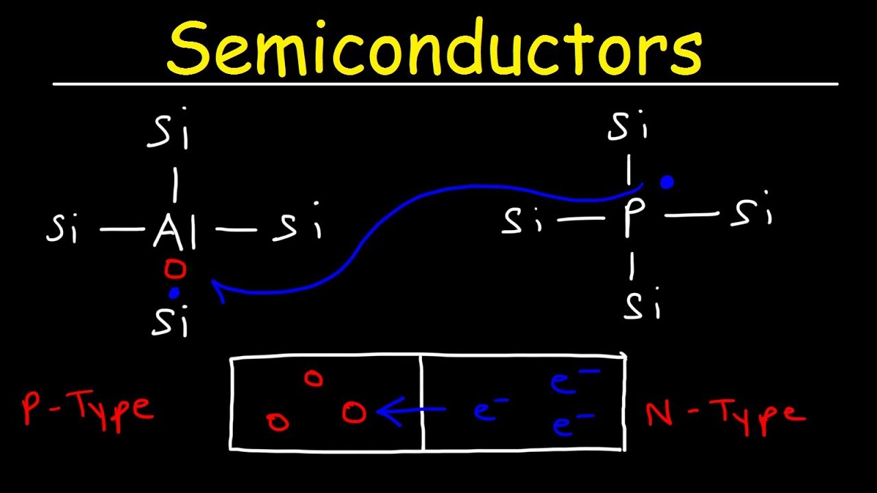
Semiconductors, Insulators & Conductors, Basic Introduction, N type vs P type Semiconductor

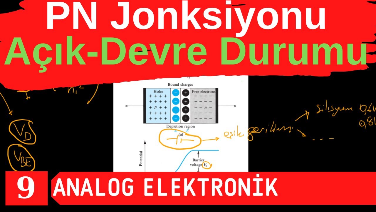
Elektronik-1 : Yarıiletken | PN Jonksiyonu-Açık Devre Durumu

Varactor (Construction & Working) Special Purpose Diode (Basic Electronics) BE/BTech 1st year

Introduction to Semiconductor Physics and Devices

V-I Characteristics of PN Junction Diode in Hindi | TECH GURUKUL By Dinesh Arya

Hoạt động của tiếp xúc P-N | Chất bán dẫn là gì?
5.0 / 5 (0 votes)