PN junction Diode Explained | Forward Bias and Reverse Bias
Summary
TLDRThis video explains the fundamentals of PN junctions in semiconductors, detailing the roles of p-type and n-type materials, their charge carriers, and the concept of the depletion region. It illustrates how applying forward or reverse bias affects current flow, with forward bias reducing the depletion width and allowing current to flow, while reverse bias increases resistance, leading to minimal current flow known as reverse saturation current. The video also addresses the impact of temperature on reverse saturation current and concludes with a caution about exceeding the breakdown voltage in reverse bias conditions.
Takeaways
- 😀 P-type semiconductors have holes as majority carriers, while n-type semiconductors have electrons as majority carriers.
- 🔌 The junction where p-type and n-type semiconductors meet is called the PN junction, which functions as a diode.
- ⚡ Doping a silicon crystal with p-type and n-type impurities creates a depletion region where free charge carriers are scarce.
- 🔋 The built-in potential at the PN junction is approximately 0.7 volts for silicon and around 0.3 volts for germanium.
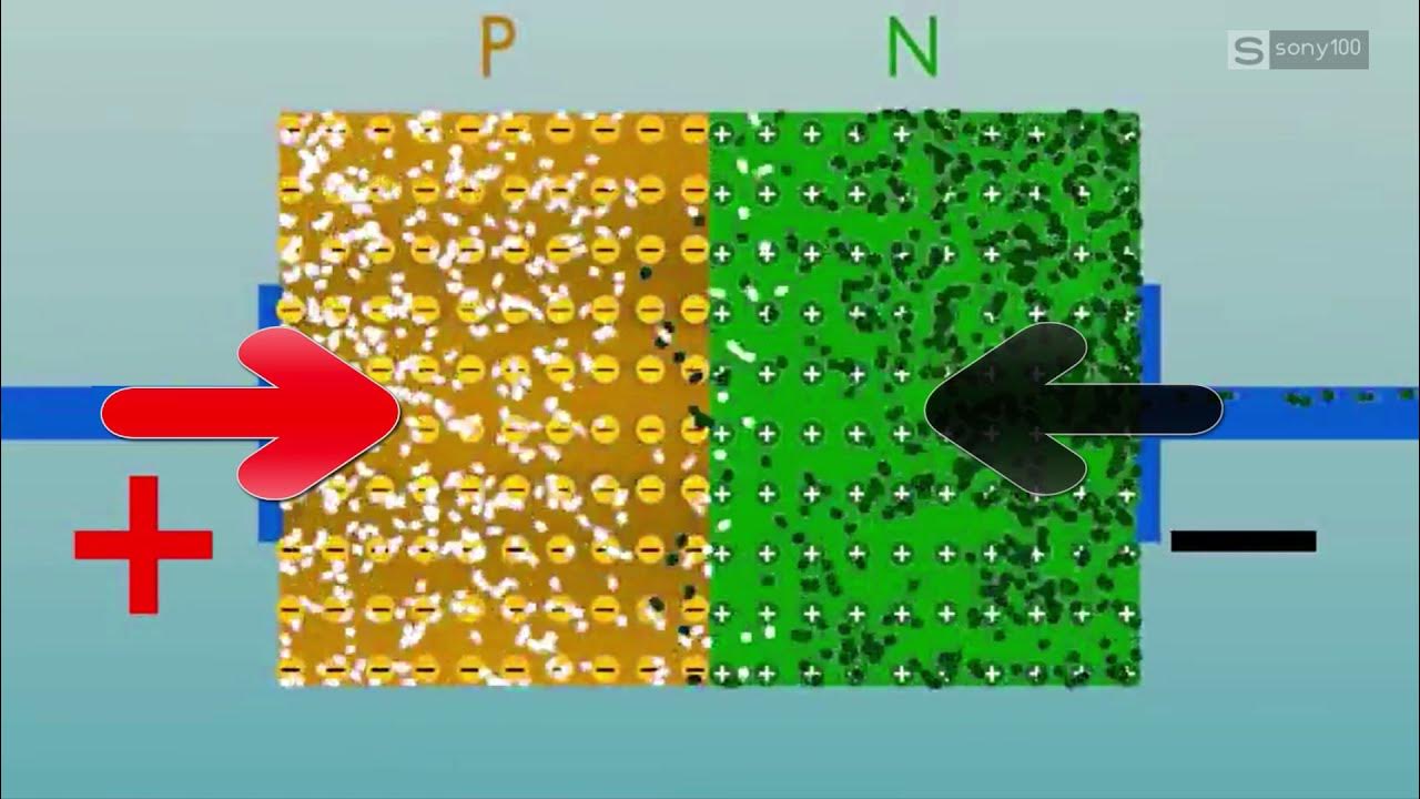
- 🔄 In forward bias, the positive terminal connects to the p-side, reducing the depletion region's width and allowing current to flow.
- ⬅️ In reverse bias, the negative terminal connects to the p-side, increasing the depletion region's width and minimizing current flow.
- 💡 Minority carriers can still cross the depletion region in reverse bias, resulting in a small reverse saturation current.
- 🌡️ The reverse saturation current increases with temperature, roughly doubling for every 10-degree rise.
- ⚠️ The diode must not exceed its breakdown voltage in reverse bias, or it will conduct heavily due to an influx of minority carriers.
- 🗨️ Engaging with the video, viewers are encouraged to leave comments, questions, and subscribe for more content.
Q & A
What are p-type and n-type semiconductors?
-P-type semiconductors have holes as majority carriers and electrons as minority carriers, while n-type semiconductors have electrons as majority carriers and holes as minority carriers.
What is a PN Junction?
-A PN Junction is formed by doping one side of a silicon crystal with a p-type impurity and the other side with an n-type impurity. It acts as a diode, where the p-type and n-type regions meet.
What happens to electrons when they diffuse from the n-type region to the p-type region?
-When electrons from the n-type region diffuse into the p-type region, they become minority carriers and recombine with holes, creating positive and negative ions near the junction.
What is the depletion region?
-The depletion region is the area near the PN Junction that is depleted of free charge carriers due to the recombination of electrons and holes, leaving behind immobile positive and negative ions.
How does the built-in electric field affect charge carriers?
-The built-in electric field points from positive ions to negative ions and prevents majority carriers from crossing the depletion region while allowing some minority carriers to cross.
What occurs during forward bias of a PN Junction?
-In forward bias, the positive terminal of the battery is connected to the p-side and the negative to the n-side, reducing the effective electric field and allowing majority carriers to cross the depletion region, leading to increased current flow.
What is reverse bias in a PN Junction?
-In reverse bias, the negative terminal of the battery is connected to the p-side and the positive to the n-side, increasing the width of the depletion region and effectively preventing the flow of majority carriers.
What is reverse saturation current?
-Reverse saturation current is the small current that flows in reverse bias due to the movement of minority carriers. It is typically in the range of microamperes to nanometers.
How does temperature affect reverse saturation current?
-As the temperature increases, the reverse saturation current increases due to more thermally generated electron-hole pairs, nearly doubling for every 10-degree rise in temperature.
What is breakdown voltage in the context of a PN Junction?
-Breakdown voltage is the maximum reverse voltage that can be applied to a PN Junction before it conducts heavily, leading to a sudden increase in current due to the appearance of many minority carriers.
Outlines

This section is available to paid users only. Please upgrade to access this part.
Upgrade NowMindmap

This section is available to paid users only. Please upgrade to access this part.
Upgrade NowKeywords

This section is available to paid users only. Please upgrade to access this part.
Upgrade NowHighlights

This section is available to paid users only. Please upgrade to access this part.
Upgrade NowTranscripts

This section is available to paid users only. Please upgrade to access this part.
Upgrade NowBrowse More Related Video

Hoạt động của tiếp xúc P-N | Chất bán dẫn là gì?

How does a Diode Work? A Simple Explanation | How Diodes Work | Electrical4U

Semiconductor PN Junctions, The Depletion Region and Diode Characteristics

Muddiest Points: Electronic Properties II

VI Characteristics of PN Junction Diode | PN Junction Forward Bias | PN Junction Reverse Bias

SE1x_2022_Week_2_6_Semiconductor_Junction-video
5.0 / 5 (0 votes)