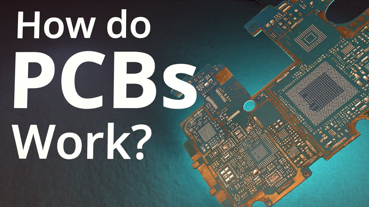
Apa Itu PCB? Proses Pembuatan PCB, Jenis dan Tipenya pada Kelas Industrial dan Hobi Elektronika
Summary
TLDRThis video explains the fundamentals of Printed Circuit Boards (PCBs), detailing their history, types, and materials used in their construction. PCBs are essential for assembling electronic components and ensuring reliable circuit connections. The script covers different PCB types, including single-layer, double-sided, and multilayer, as well as flexible and rigid variants. It also explores the materials like FR4 and SS2, solder masks, and silkscreen layers. Additionally, it highlights the advantages of modern PCB manufacturing, allowing anyone from amateurs to professionals to design high-quality, industry-standard PCBs at affordable prices.
Takeaways
- 😀 PCBs (Printed Circuit Boards) are essential in electronic circuits, ranging from simple to complex devices, helping to connect electronic components.
- 😀 The concept of PCB was introduced by an Austrian scientist named Paul Eisler in 1936, and it was first used in radio circuits.
- 😀 The use of PCBs expanded in the 1940s, with the United States adopting them for military radios and later for commercial products after World War II.
- 😀 PCB structures are similar to layered cakes, composed of substrates, copper layers, solder masks, and silkscreens.
- 😀 The most common PCB substrates are SS2 (paper-based) and FR4 (fiberglass-based), with FR4 being known for its low water absorption and high heat resistance.
- 😀 Copper layers on PCBs are thin and bonded to the substrate through heat. Single-sided, double-sided, and multilayer PCBs all use different configurations of these layers.
- 😀 Solder masks are thin protective layers that prevent accidental contact with conductive paths, helping prevent shorts or faulty connections.
- 😀 Silkscreen layers, usually white or black, are used to mark component symbols and positions on the PCB, making assembly easier and more precise.
- 😀 PCBs can be classified into three types based on the number of layers: single-sided, double-sided, and multilayer.
- 😀 There are three flexibility categories for PCBs: rigid (made from solid materials like fiberglass), flexible (made from materials like polyamide), and rigid-flex (a hybrid of both).
- 😀 Aluminium PCBs are used for high-heat applications like LED lighting, as aluminium efficiently dissipates heat and is cost-effective.
Q & A
What is a PCB, and what is its primary function?
-PCB stands for 'Printed Circuit Board.' Its primary function is to connect and support electronic components by providing conductive paths for electricity, making it possible to build and organize complex electronic circuits efficiently.
Who invented the PCB, and when was it first used?
-The PCB was invented by Austrian scientist Paul Eisler in 1936. He first used it in a radio circuit. Later, in 1943, the United States adopted PCB technology for military radios, and in 1948, it began to be used in commercial products.
What are the main layers in a PCB?
-The main layers in a PCB include the substrate (base material), copper layer (conductive paths), solder mask (protective coating), and silkscreen (for component identification). The copper layer can be one-sided, double-sided, or multi-layered, depending on the PCB design.
What are the common materials used for the substrate in PCBs?
-The most common substrate materials for PCBs are SS2 and FR4. SS2 is a paper-based material with resin, while FR4 is a fiberglass-based material coated with epoxy resin. FR4 offers better insulation, lower moisture absorption, and can withstand higher temperatures.
What is the function of the solder mask on a PCB?
-The solder mask is a thin layer applied over the copper traces on a PCB to protect them from accidental contact and short circuits. It helps users solder components more precisely and prevents unintended connections. The solder mask is usually green but can also be other colors.
What does the silkscreen layer on a PCB contain?
-The silkscreen layer on a PCB contains printed symbols, numbers, and letters. These serve as indicators for the placement of components and are crucial for assembly, making it easier to identify components and ensure correct soldering.
What are the different types of PCBs based on the number of layers?
-PCBs are classified into three types based on the number of layers: single-sided, double-sided, and multi-layered. Single-sided PCBs have a single layer of conductive material, double-sided PCBs have conductive layers on both sides, and multi-layer PCBs contain multiple conductive layers stacked together.
What are the advantages of multi-layer PCBs?
-Multi-layer PCBs are compact and allow for higher circuit density, which is ideal for complex electronic devices. They provide better performance for high-speed circuits, greater flexibility in design, and more robust mechanical strength.
What are rigid, flexible, and rigid-flex PCBs?
-Rigid PCBs are made from solid, inflexible materials like fiberglass. Flexible PCBs are made from pliable materials like polyimide, allowing them to bend without damaging the circuit. Rigid-flex PCBs combine both rigid and flexible materials, offering the advantages of both types.
What is the role of aluminum PCBs, and where are they typically used?
-Aluminum PCBs are designed to efficiently dissipate heat. They are commonly used in applications where high heat generation is a concern, such as LED lighting. The aluminum backing helps distribute heat evenly, preventing overheating and ensuring the circuit's longevity.
Outlines

Этот раздел доступен только подписчикам платных тарифов. Пожалуйста, перейдите на платный тариф для доступа.
Перейти на платный тарифMindmap

Этот раздел доступен только подписчикам платных тарифов. Пожалуйста, перейдите на платный тариф для доступа.
Перейти на платный тарифKeywords

Этот раздел доступен только подписчикам платных тарифов. Пожалуйста, перейдите на платный тариф для доступа.
Перейти на платный тарифHighlights

Этот раздел доступен только подписчикам платных тарифов. Пожалуйста, перейдите на платный тариф для доступа.
Перейти на платный тарифTranscripts

Этот раздел доступен только подписчикам платных тарифов. Пожалуйста, перейдите на платный тариф для доступа.
Перейти на платный тарифПосмотреть больше похожих видео


5.0 / 5 (0 votes)
