Closed loop control of Phase-Shifted Full bridge DC-DC Converter in MATLAB/Simulink!
Summary
TLDRIn this video, Sankashan Duggar Prasad demonstrates how to design and simulate a phase-shifted full-bridge DC-DC converter. The process includes detailed calculations for transformer turns ratio, inductance, and capacitance, with input and output parameters specified for the converter. The simulation setup uses MOSFETs, a linear transformer, and diodes, controlled by PWM signals generated through a PI controller. The video shows how to achieve a stable 12V output and discusses the impact of varying reference voltages. It offers a thorough guide for those interested in designing and simulating efficient DC-DC converters.
Takeaways
- 😀 The video demonstrates how to simulate and design a phase-shifted full bridge DC-to-DC converter.
- 😀 The design includes a circuit diagram showing the operation of a DC-to-AC converter, using switches and transformers.
- 😀 Key design parameters include an input voltage of 600V, an output voltage of 12V, and a required output power of 480W.
- 😀 The switching frequency is set at 250kHz, and the maximum current ripple is 20% of the load current.
- 😀 The transformer turns ratio is calculated as 0.025, based on the input-output voltage ratio.
- 😀 The inductor value is calculated to be 0.6 µH, using the voltage across the inductor, duty cycle, and ripple current.
- 😀 The capacitor value is calculated as 106.666 µF, based on the ripple current and voltage ripple.
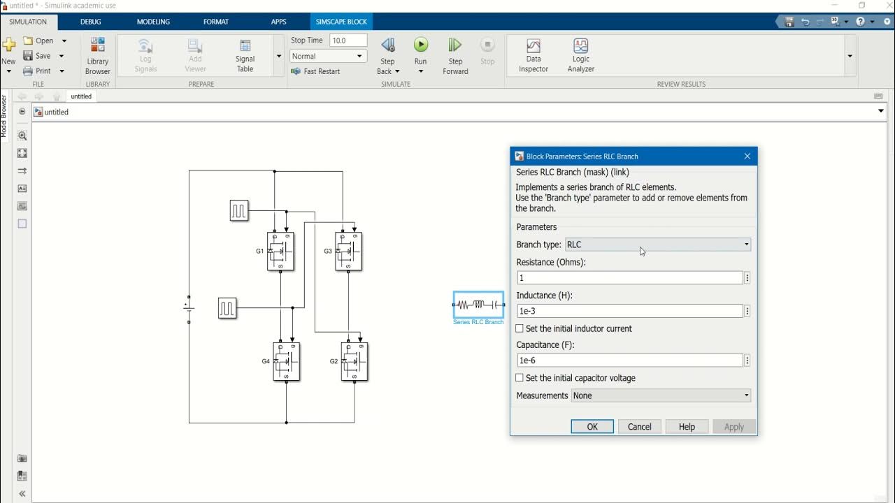
- 😀 The simulation setup includes MOSFETs, a linear transformer, diodes, and a series RLC branch for inductance and capacitance values.
- 😀 A PID controller is used to regulate the output voltage, with the reference voltage set to 12V.
- 😀 The final simulation output should be around 12V, and experimenting with voltage reference settings can improve accuracy.
Q & A
What is the primary focus of the video?
-The video focuses on simulating and designing a phase-shifted full-bridge DC-DC converter, with detailed explanations of the design, simulation steps, and component calculations.
What are the input design parameters for the converter?
-The input design parameters include a 600V input voltage, 12V output voltage, 480W required output power, 40A load current, a switching frequency of 250kHz, and a current ripple of a maximum of 20%.
How does the phase-shifted full-bridge converter work in the video?
-The converter uses MOSFET switches to alternately conduct during the positive and negative half-cycles of AC, creating a transformer output which is then rectified back to DC to power the load.
What is the significance of the voltage drop across the inductor and switches?
-The voltage drop across the inductor and switches is critical to accurately determine the output voltage. The design compensates for the voltage drop by adjusting the desired output voltage to 15V, despite aiming for 12V.
How is the inductance value calculated in the design?
-The inductance is calculated using the formula L = V_L * Δt / ΔI, where V_L is the voltage across the inductor, Δt is the duty cycle time, and ΔI is the current ripple. The calculated value is 0.6 microhenry.
How is the capacitance value determined in the simulation?
-Capacitance is determined using the formula C = I_ripple * Δt / ΔV, where I_ripple is the current ripple, Δt is the duty cycle time, and ΔV is the voltage ripple. The calculated value is 106.666 microfarads.
What is the purpose of the PI controller in the simulation?
-The PI controller ensures that the output voltage stays close to the desired value by adjusting the PWM signals based on the difference between the reference voltage and the measured output voltage.
What components are used to create the full-bridge converter in the simulation?
-The components used include MOSFETs as the switching devices, a linear transformer for isolation, diodes for the rectifier, inductors and capacitors for filtering, and a PI controller to regulate the output.
Why is a linear transformer used in the simulation?
-A linear transformer is used to isolate the two circuits (DC side and AC side) and adjust voltage levels appropriately. The transformer also provides the necessary impedance matching for the simulation.
What is the role of the clock in the simulation setup?
-The clock drives the switching pulses for the MOSFETs. It controls the switching frequency and ensures that the timing of the PWM signals aligns with the designed switching behavior of the converter.
Outlines

このセクションは有料ユーザー限定です。 アクセスするには、アップグレードをお願いします。
今すぐアップグレードMindmap

このセクションは有料ユーザー限定です。 アクセスするには、アップグレードをお願いします。
今すぐアップグレードKeywords

このセクションは有料ユーザー限定です。 アクセスするには、アップグレードをお願いします。
今すぐアップグレードHighlights

このセクションは有料ユーザー限定です。 アクセスするには、アップグレードをお願いします。
今すぐアップグレードTranscripts

このセクションは有料ユーザー限定です。 アクセスするには、アップグレードをお願いします。
今すぐアップグレード関連動画をさらに表示
Design of DC AC Converter Using MATLAB SIMULINK

Simulation of a Dual Active Bridge Converter in MATLAB | SIMULINK

entrance into the DC DC Converter Basic Topologies
How does a Battery Charger work? CCCV Battery Charging | CCCV regulator | Li-ion cell charger

Lec 53: Example of Transformer Design
Battery driven Electric vehicle with regenerative Braking operation | Electric vehicle Simulation |
5.0 / 5 (0 votes)
