Introduction to Scanning Electron Microscopy (SEM)
Summary
TLDRWes Auker, a Research Technologist at Penn State, provides an introduction to Scanning Electron Microscopy (SEM). SEM uses a focused electron beam to gather data on sample morphology, chemical composition, and crystalline structure. The technique generates 2D images and is useful for surface morphology, elemental contrast, and chemical composition analysis. Applications include EDS for composition analysis and EBSD for crystal orientation. SEM is valued for its rapid results, ease of use, and ability to analyze from macro to nanostructures, though it has limitations in surface analysis compared to other techniques like Auger Spectroscopy.
Takeaways
- 🔬 Scanning Electron Microscopy (SEM) uses a focused beam of high-energy electrons to generate signals from a solid specimen's surface.
- 📏 SEM reveals critical information about a sample, including its morphology, chemical composition, and crystalline structure.
- 🖼️ SEM generates 2D images that display spatial variations in surface properties based on electron interactions.
- ⚛️ SEM can perform qualitative and quantitative compositional analysis using EDS (Energy Dispersive Spectroscopy) and crystalline analysis using EBSD (Electron Backscatter Diffraction).
- 💡 The interaction volume of SEM varies depending on the accelerating voltage and materials, extending from under 100 nanometers to 5 microns into the surface.
- 🌀 Low-energy secondary electrons, ejected from conduction or valence bands, are commonly used for imaging in SEM.
- 📊 SEM applications include surface morphology, elemental contrast, phase structure analysis, and chemical composition mapping.
- 📈 Back-scattered electron imaging in SEM helps identify materials by atomic number, with brighter features indicating higher atomic numbers.
- ⚙️ SEM offers advantages like fast results, flexibility in sample sizes, and ease of user training but is not a true surface technique compared to Auger Spectroscopy or XPS.
- 🚀 Technical specifications include sub-nanometer resolution, an interaction volume range from 50 nanometers to 5 microns, and gun voltage from 250V to 30kV.
Q & A
What is the primary function of a Scanning Electron Microscope (SEM)?
-A Scanning Electron Microscope (SEM) uses a focused beam of high-energy electrons to generate signals at the surface of solid specimens. These signals reveal information about the sample, including its morphology, chemical composition, crystalline structure, and orientation.
What types of information can SEM imaging provide about a sample?
-SEM imaging provides information on surface morphology, chemical composition, crystalline structure, and crystal orientations of materials that make up the sample.
How are 2-dimensional images generated in SEM analysis?
-In most SEM applications, data are collected over a selected area of the sample's surface, and 2-dimensional images are generated that display spatial variations in the properties of the sample.
What are some specialized analysis techniques used in SEM?
-Specialized SEM techniques include Energy Dispersive X-ray Spectroscopy (EDS) for chemical composition analysis, and Electron Backscatter Diffraction (EBSD) for determining crystalline structure and crystal orientations.
What is the 'interaction volume' in the context of SEM?
-The 'interaction volume' refers to the region where primary electron beams interact with the sample, losing energy through random scattering and absorption. This volume extends from less than 100 nanometers up to 5 microns into the sample surface, depending on factors like accelerating voltage and material.
What is the significance of secondary electrons in SEM imaging?
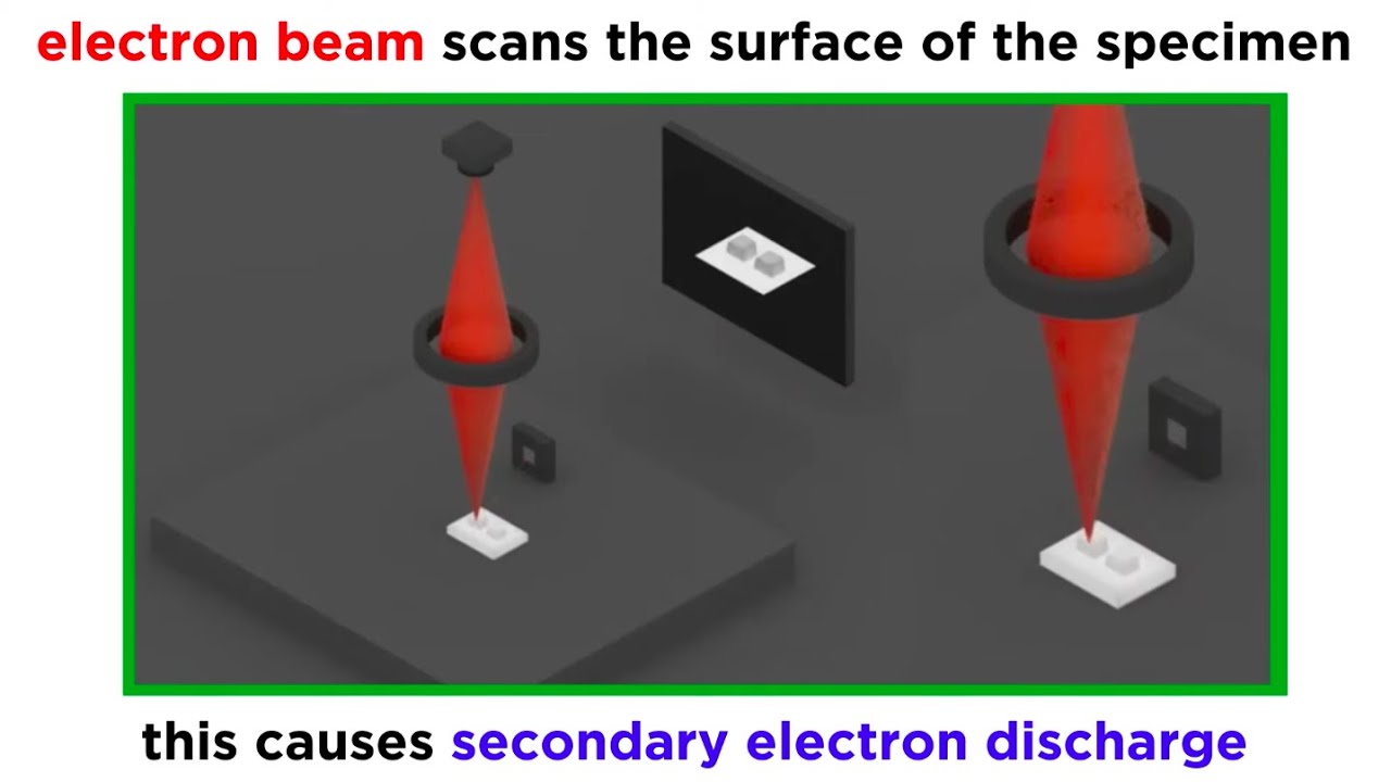
-Secondary electrons, which have low energy (less than 50 eV), are commonly used for imaging in SEM. These electrons are ejected from the sample's conduction or valence bands through inelastic scattering with beam electrons and originate from just a few nanometers below the sample surface.
What are some common applications of SEM?
-Common SEM applications include surface morphology, elemental contrast, chemical composition analysis, phase structure analysis, fracture analysis, surface contamination studies, semiconductor inspection, and grain structure analysis.
How do backscattered electron images differ from secondary electron images?
-Backscattered electron images are based on the atomic number of the scanned material. Higher atomic numbers produce brighter features, while lower atomic numbers result in darker features in the image.
What are some advantages of using SEM?
-Advantages of SEM include fast results for analyzing various sample sizes (from small powders to large wafers), ease of user training, and the ability to analyze materials at macro, micro, and nanoscales.
What are some disadvantages of SEM compared to other surface techniques?
-Compared to techniques like Auger Spectroscopy or X-ray Photoelectron Spectroscopy (XPS), SEM is not a true surface technique because the interaction volume extends beyond the surface, typically greater than 10 nanometers. Additionally, SEM often requires dry samples and may need standards for quantitative analysis.
Outlines

このセクションは有料ユーザー限定です。 アクセスするには、アップグレードをお願いします。
今すぐアップグレードMindmap

このセクションは有料ユーザー限定です。 アクセスするには、アップグレードをお願いします。
今すぐアップグレードKeywords

このセクションは有料ユーザー限定です。 アクセスするには、アップグレードをお願いします。
今すぐアップグレードHighlights

このセクションは有料ユーザー限定です。 アクセスするには、アップグレードをお願いします。
今すぐアップグレードTranscripts

このセクションは有料ユーザー限定です。 アクセスするには、アップグレードをお願いします。
今すぐアップグレード関連動画をさらに表示

Introduction to the Scanning Electron Microscope (SEM)

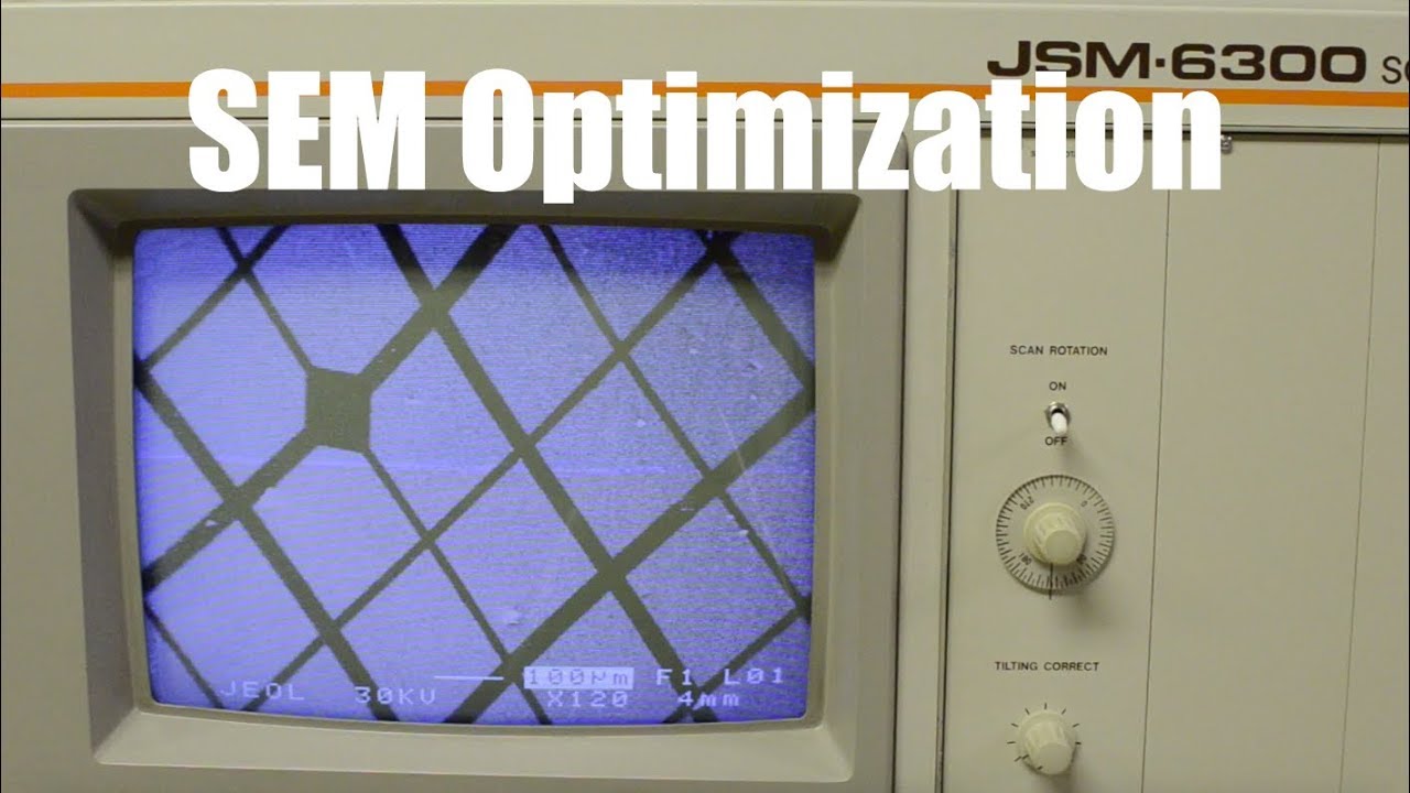
SEM Optimization, Astigmatism Correction, and Basic Electron Optics

Pengujian Alat SEM - Scanning Electron Microscope

Electron Microscopy (TEM and SEM)

Temp1 Cap1 Epi3 Microscopía Electrónica

Scanning Electron Microscopy (SEM) | Working Principles and application of SEM in biology
5.0 / 5 (0 votes)
