Common-Base Configuration of a Transistor
Summary
TLDRThis lecture explains the common base configuration of a transistor, focusing on its operation and key equations. It covers the transistor's three terminals—emitter, base, and collector—and how the base is common to both the input and output circuits. The lecture describes the forward and reverse biasing of the junctions, the current flow directions, and the relationships between the emitter, base, and collector currents. Key concepts such as Kirchhoff's Current Law and the common base current gain (α) are discussed, emphasizing the transistor's ability to amplify weak signals in active mode.
Takeaways
- 😀 A transistor is a three-terminal device with the base, emitter, and collector as its key components.
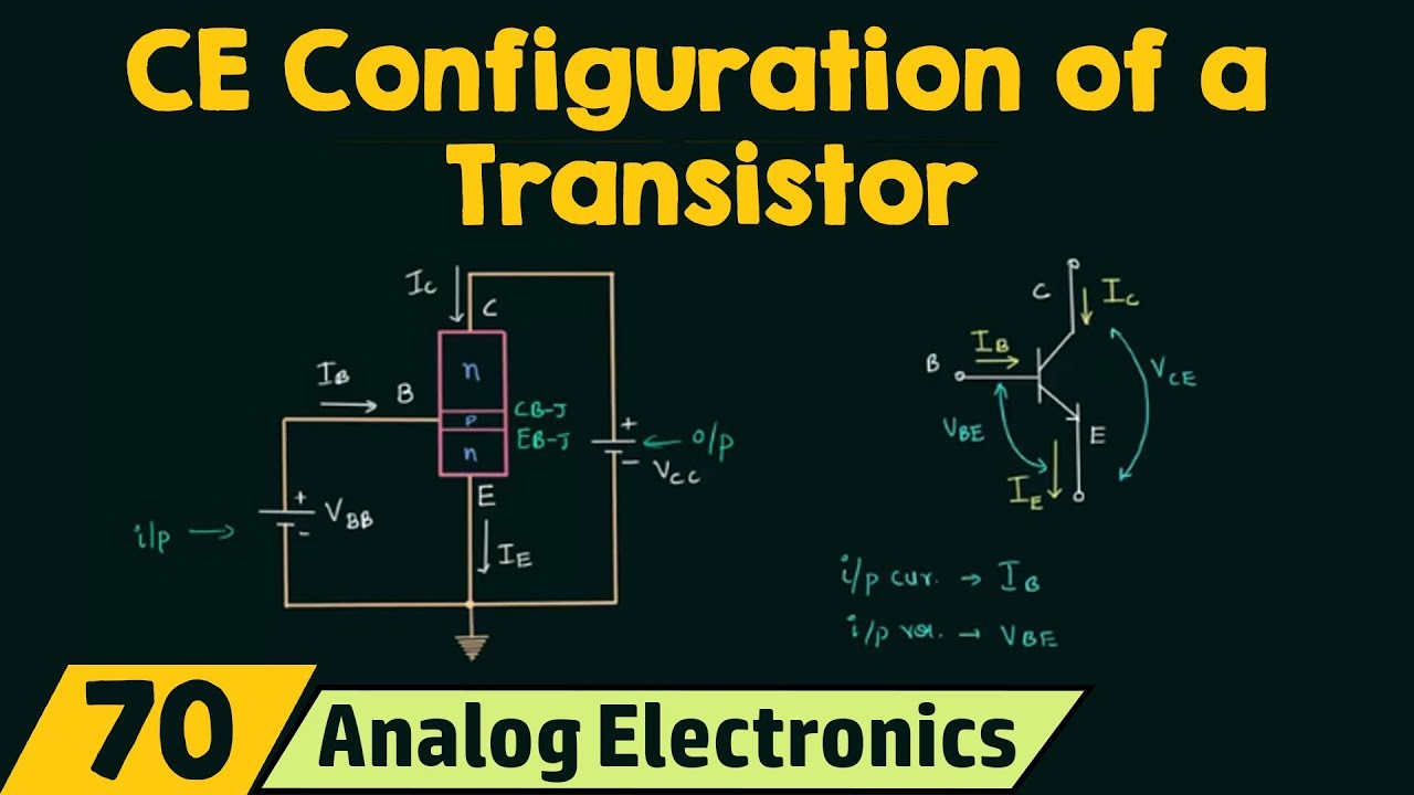
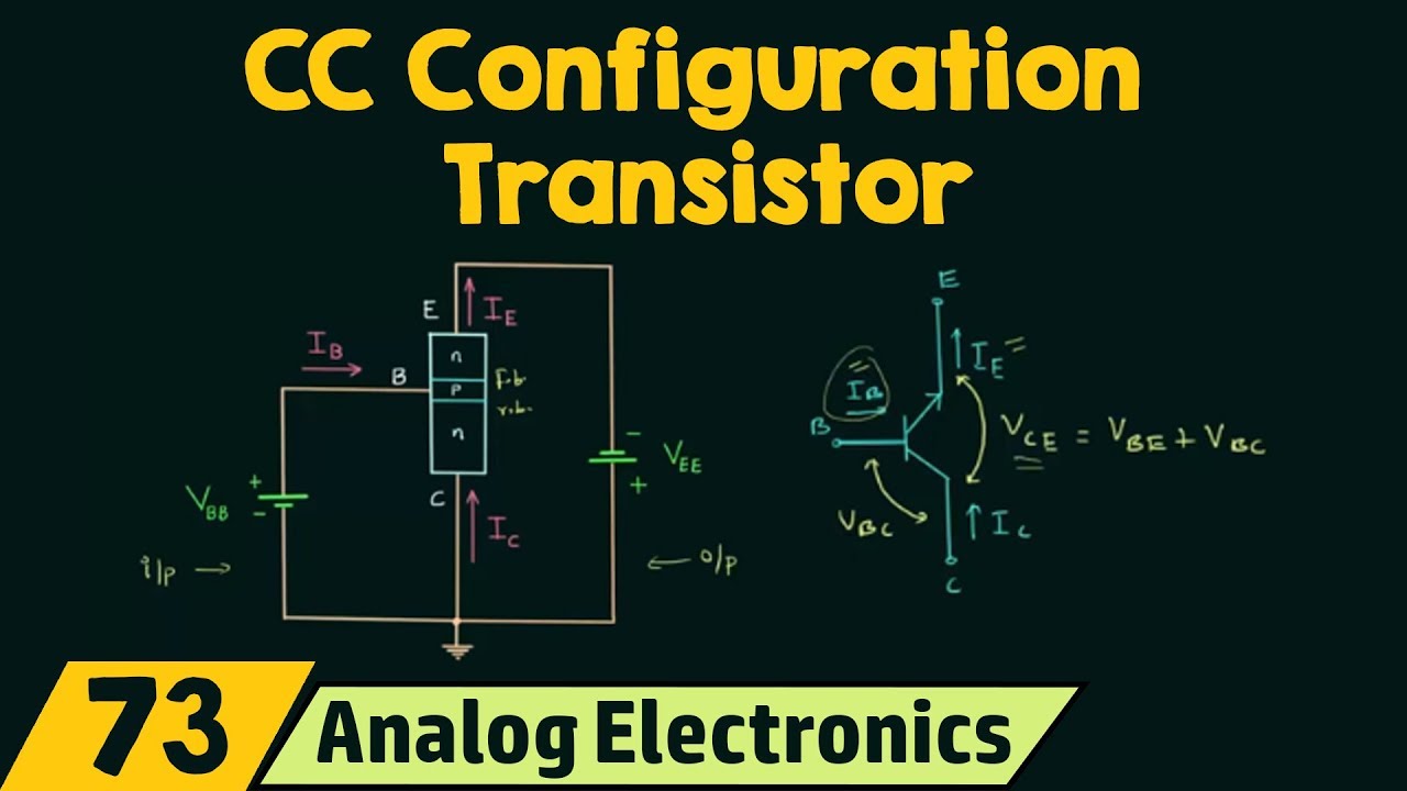
- 😀 The three common transistor configurations are common base, common emitter, and common collector, with common emitter being the most widely used.
- 😀 In the common base configuration, the base is common to both the input and output circuits, and it is grounded.
- 😀 The transistor operates in active mode to amplify weak signals, where the base-emitter junction is forward biased, and the collector-base junction is reverse biased.
- 😀 In the active mode, the transistor behaves like two diodes connected back-to-back: the base-emitter junction is forward biased, and the collector-base junction is reverse biased.
- 😀 The relationship between the emitter current (I_E), base current (I_B), and collector current (I_C) is governed by Kirchhoff's Current Law: I_E = I_B + I_C.
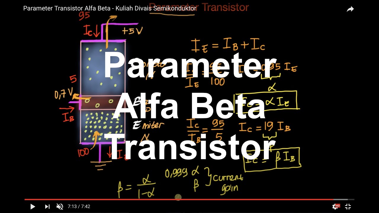
- 😀 The collector current (I_C) is related to the emitter current (I_E) by the factor alpha (α), where α = I_C / I_E, and typically ranges from 0.95 to 0.98.
- 😀 Alpha (α) represents the current gain in the common base configuration, indicating that most of the emitter current is transferred to the collector.
- 😀 The reverse saturation current (I_CBO) is a small current that can generally be neglected in the common base configuration, as it is caused by minority charge carriers.
- 😀 The voltage across the base-emitter junction (V_BE) and the voltage across the collector-base junction (V_CB) are important for understanding transistor operation and should be labeled correctly according to proper nomenclature.
Q & A
What are the three terminals of a transistor?
-The three terminals of a transistor are the Base, Emitter, and Collector.
What are the three main transistor configurations?
-The three main transistor configurations are Common Base, Common Emitter, and Common Collector.
Which transistor configuration is most commonly used and why?
-The Common Emitter configuration is most commonly used due to its various advantages, such as higher voltage and current gain.
How is the Common Base configuration different from the others?
-In the Common Base configuration, the Base terminal is common to both the input and output circuits and is typically grounded.
What happens in a transistor when it operates in active mode?
-In active mode, the transistor amplifies a weak input signal. The Emitter-Base junction is forward biased, and the Base-Collector junction is reverse biased.
How are the two junctions in a transistor biased in active mode?
-In active mode, the Emitter-Base junction (Junction J1) is forward biased, and the Base-Collector junction (Junction J2) is reverse biased.
What is the significance of the term 'reverse saturation current' (Icbo)?
-Icbo refers to the reverse saturation current in the Base-Collector junction when the Emitter is open. It is typically very small and can often be neglected in calculations.
What is the relationship between the Emitter current (Ie) and the Collector current (Ic)?
-The relationship between the Emitter and Collector currents is given by Ic = α * Ie, where α is the common base current gain, typically between 0.95 and 0.98.
What does the current gain (α) represent in the Common Base configuration?
-The current gain (α) represents the ratio of the Collector current (Ic) to the Emitter current (Ie) in the Common Base configuration, typically ranging from 0.95 to 0.98.
Why is it important to follow the correct nomenclature for transistor voltages, such as Vbe and Vcb?
-The correct nomenclature ensures proper understanding of the voltage potentials across the transistor terminals. Vbe and Vcb indicate the voltage difference between the Base and Emitter, and the Base and Collector, respectively, with the higher potential listed first.
Outlines

Cette section est réservée aux utilisateurs payants. Améliorez votre compte pour accéder à cette section.
Améliorer maintenantMindmap

Cette section est réservée aux utilisateurs payants. Améliorez votre compte pour accéder à cette section.
Améliorer maintenantKeywords

Cette section est réservée aux utilisateurs payants. Améliorez votre compte pour accéder à cette section.
Améliorer maintenantHighlights

Cette section est réservée aux utilisateurs payants. Améliorez votre compte pour accéder à cette section.
Améliorer maintenantTranscripts

Cette section est réservée aux utilisateurs payants. Améliorez votre compte pour accéder à cette section.
Améliorer maintenantVoir Plus de Vidéos Connexes

Common-Emitter Configuration of a Transistor

Parameter Transistor Alfa Beta | Kuliah Fisika Semikonduktor

Common Emitter Configuration with input and output characteristics in Telugu//EC&PS//diploma//B.tech

L39 | Emitter Coupled Logic | Digital System Design (KEC302) | Hindi

Electrical Engineering: Ch 3: Circuit Analysis (28 of 37) Current Graph for NPN BJT Transistor

Common-Collector Configuration of a Transistor
5.0 / 5 (0 votes)
