Common Base configuration with input and output characteristics in Telugu/EC&PS/diploma//engineering
Summary
TLDRThis video provides a comprehensive explanation of the **Common Base Transistor Configuration** for diploma students in Electronics and Communication. The focus is on understanding the transistor's three key terminals—Emitter, Base, and Collector—and their role in input and output circuits. The video covers how to calculate input and output resistances, and discusses the input and output characteristics curves. It also explains the transistor's behavior in different operating regions: Active, Saturation, and Cut-off. The session concludes with a look at how PNP transistors function in the common base configuration, setting the stage for further exploration of other configurations.
Takeaways
- 😀 Common Base, Common Emitter, and Common Collector are the three primary transistor configurations.
- 😀 In a Common Base configuration, the base terminal is connected to ground and serves as the common terminal for both input and output.
- 😀 A PNP transistor has three terminals: Emitter, Base, and Collector, with the base being the common terminal.
- 😀 The input characteristics curve represents the relationship between the Emitter current (I_E) and the Emitter-Base voltage (V_BE) at a constant Collector-Base voltage (V_CB).
- 😀 The formula for calculating input resistance (R_I) in the Common Base configuration is: R_I = ΔV_BE / ΔI_E (at constant V_CB).
- 😀 The output characteristics curve shows the relationship between the Collector current (I_C) and the Collector-Base voltage (V_CB) at a constant Emitter current (I_E).
- 😀 The formula for calculating output resistance (R_O) in the Common Base configuration is: R_O = ΔV_CB / ΔI_C (at constant I_E).
- 😀 The transistor operates in three distinct regions: Active, Saturation, and Cutoff, depending on the biasing of the junctions.
- 😀 In the Active region, the Base-Emitter junction is forward biased, and the Collector-Base junction is reverse biased.
- 😀 In the Saturation region, both junctions (Base-Emitter and Collector-Base) are forward biased.
- 😀 In the Cutoff region, both junctions (Base-Emitter and Collector-Base) are reverse biased, and the transistor is turned off.
Q & A
What are the three main types of transistor configurations?
-The three main types of transistor configurations are Common Base, Common Emitter, and Common Collector.
What is the key characteristic of the Common Base configuration?
-In the Common Base configuration, the Base terminal is common to both the input and output, and it is typically connected to ground.
Which terminals of a transistor are involved in the Common Base configuration?
-The three terminals involved in the Common Base configuration are the Emitter, Base, and Collector.
What does the term 'input current' refer to in the Common Base configuration?
-The input current in the Common Base configuration refers to the Emitter current, denoted as I_E.
What does 'V_BE' represent in the Common Base configuration?
-'V_BE' represents the voltage between the Base and Emitter terminals in the Common Base configuration.
What does the curve of the Input Characteristics represent?
-The Input Characteristics curve represents the relationship between the Emitter current (I_E) and the Base-Emitter voltage (V_BE) at a constant Collector-Base voltage (V_CB).
What does the Output Characteristics curve illustrate?
-The Output Characteristics curve illustrates the relationship between the Collector current (I_C) and the Collector-Base voltage (V_CB), with the Emitter current held constant.
How is the Input Resistance in the Common Base configuration calculated?
-The Input Resistance (R_I) is calculated using the formula: R_I = ΔV_BE / ΔI_E at constant V_CB, which gives the ratio of change in voltage to change in current at a fixed Collector-Base voltage.
What is the significance of the biasing of the transistor in the Common Base configuration?
-The biasing of the transistor determines its operating region: the Active Region (input junction forward-biased, output junction reverse-biased), Saturation Region (both junctions forward-biased), and Cut-Off Region (both junctions reverse-biased).
How do the input and output voltages affect the operation of a transistor in the Common Base configuration?
-The input voltage (V_BE) controls the emitter current, while the output voltage (V_CB) controls the collector current. Both influence the transistor's behavior, determining whether it operates in the Active, Saturation, or Cut-Off regions.
Outlines

This section is available to paid users only. Please upgrade to access this part.
Upgrade NowMindmap

This section is available to paid users only. Please upgrade to access this part.
Upgrade NowKeywords

This section is available to paid users only. Please upgrade to access this part.
Upgrade NowHighlights

This section is available to paid users only. Please upgrade to access this part.
Upgrade NowTranscripts

This section is available to paid users only. Please upgrade to access this part.
Upgrade NowBrowse More Related Video

Common Emitter Configuration with input and output characteristics in Telugu//EC&PS//diploma//B.tech

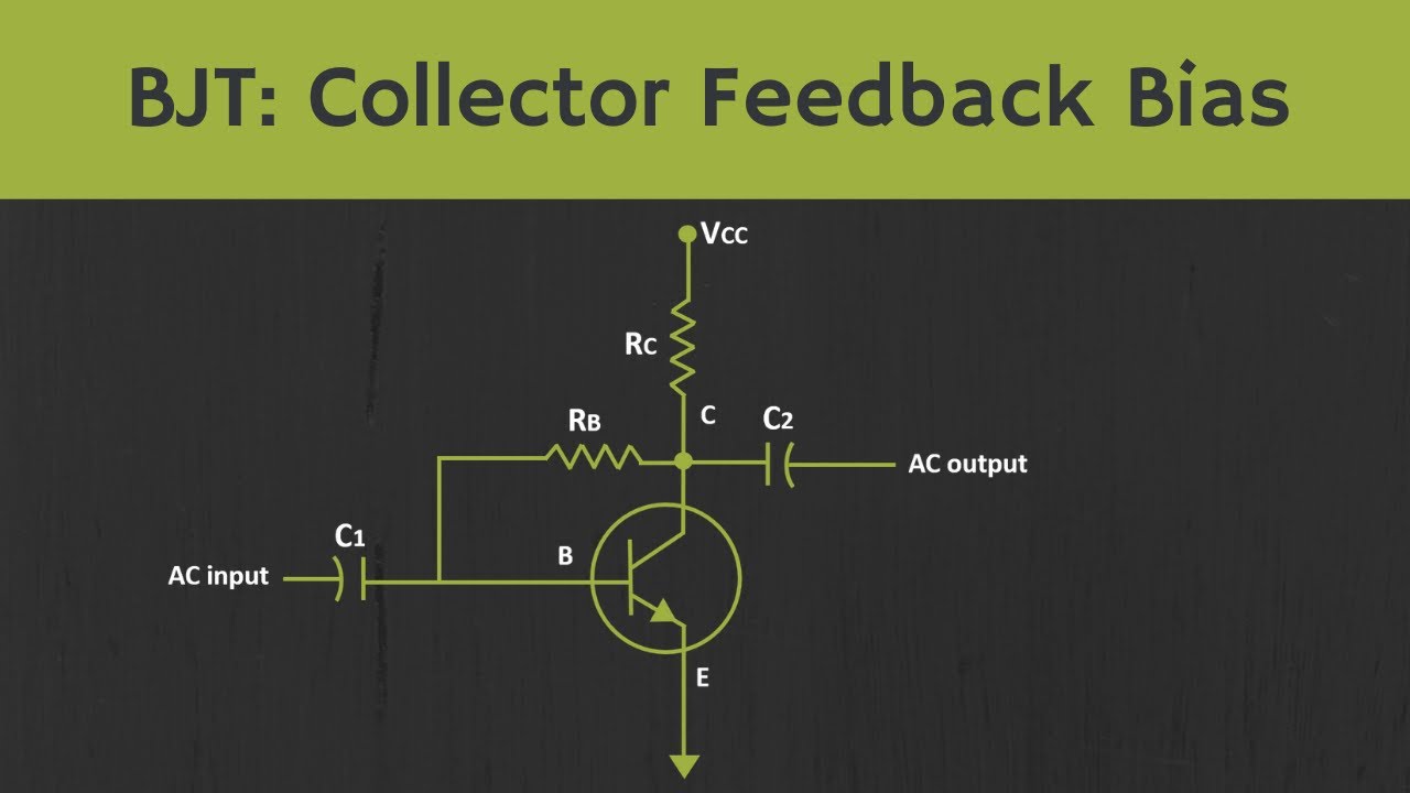
BJT: Collector Feedback Bias Explained

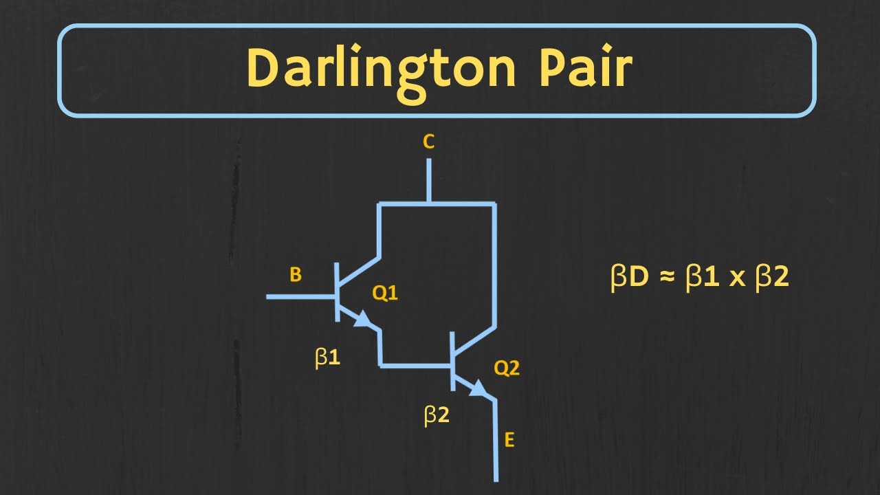
Darlington Pair Explained | The Darlington Pair as a Switch

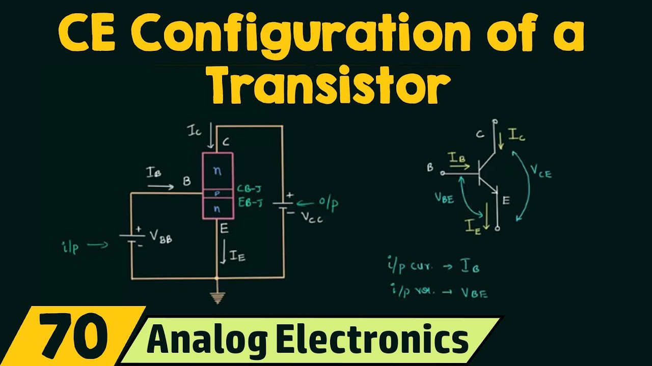
Common-Emitter Configuration of a Transistor

Dasar Elektronika : Transistor

Transistor Characteristics (CE Transistor) Basic Electronics (BJT) BE/Btech 1st year| in हिन्दी
5.0 / 5 (0 votes)