Cara Kerja Dioda PN Junction | Kuliah Fisika Semikonduktor
Summary
TLDRThis video explains the working principles of a PN Junction diode in both forward and reverse bias modes. In forward bias, a potential difference greater than 0.7 volts is applied, allowing current to flow through the PN Junction as it overcomes the built-in potential barrier. In reverse bias, the polarity is reversed, causing a depletion layer to form at the junction, preventing current flow. The video highlights the behavior of electrons and holes in each mode and their interaction with the electric field, emphasizing how the diode controls current flow.
Takeaways
- 📘 The video discusses how a PN Junction diode operates, focusing on forward and reverse bias modes.
- 🔋 In forward bias, the P-side is connected to a positive voltage, and the N-side is connected to a negative voltage.
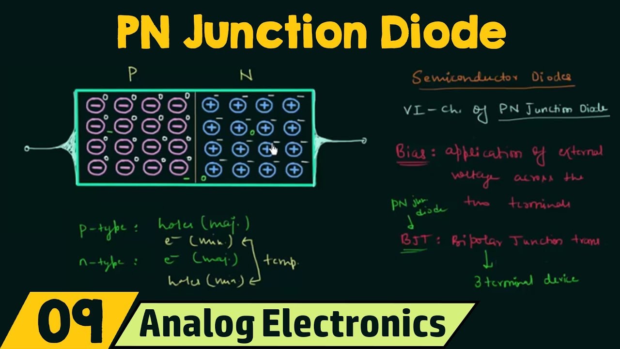
- ⚡ Before applying a forward bias, the diode has a built-in potential barrier due to positive and negative charges on the P and N sides, respectively.
- 🧮 The built-in potential is usually around 0.7 volts, which the forward voltage must exceed for current to flow.
- 💡 Once the applied forward voltage exceeds the potential barrier, current flows from the positive to the negative side through the PN junction.
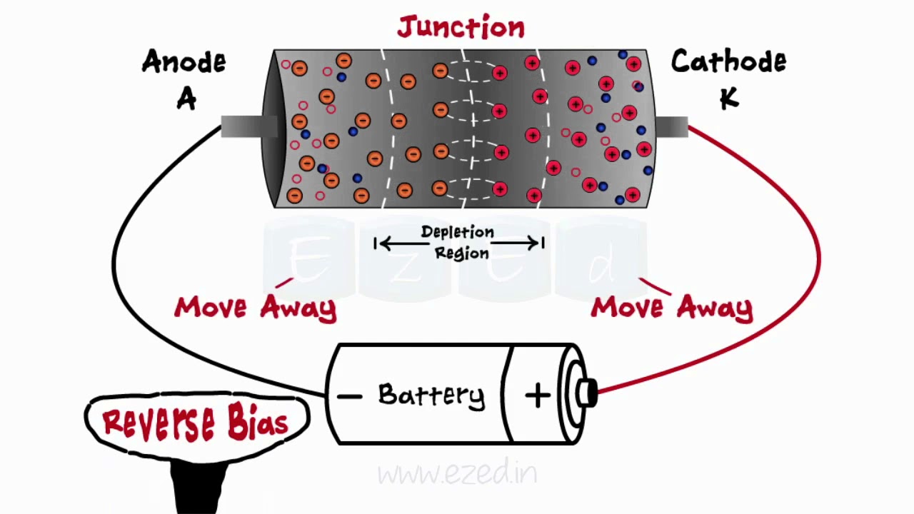
- 🔄 In reverse bias mode, the P-side is connected to a negative voltage, and the N-side to a positive voltage.
- 🌀 Under reverse bias, the positive charge on the N-side attracts electrons, leaving a positive ion charge near the junction.
- 🛑 In reverse bias, a depletion layer forms at the junction, preventing current from flowing through the diode.
- 🌐 The depletion layer in reverse bias mode acts as an insulator, stopping the movement of electrons across the junction.
- 🔍 The video emphasizes that forward bias allows current to flow, while reverse bias blocks it due to the depletion layer.
Q & A
What is the function of a PN Junction diode?
-A PN Junction diode controls the flow of current. It allows current to flow in one direction when forward biased and blocks it when reverse biased.
What is the 'forward bias' mode in a PN Junction diode?
-In forward bias mode, the positive terminal is connected to the P-side and the negative terminal to the N-side, allowing current to flow once the voltage exceeds the built-in potential of the diode.
What happens in a PN Junction diode under 'reverse bias'?
-In reverse bias mode, the positive terminal is connected to the N-side, and the negative terminal to the P-side, creating a depletion layer at the junction that prevents current from flowing.
What is the built-in potential of a PN Junction diode in forward bias?
-The built-in potential, also known as the barrier potential, is typically around 0.7 volts for silicon diodes, which must be exceeded for current to flow in forward bias.
How does the depletion layer form in reverse bias?
-In reverse bias, electrons from the N-side are pulled towards the positive terminal, and holes from the P-side are pulled towards the negative terminal, creating a depletion layer of immobile ions at the junction that blocks current.
Why does current flow in forward bias but not in reverse bias?
-In forward bias, the applied voltage reduces the depletion layer, allowing current to flow. In reverse bias, the depletion layer widens, preventing current from passing through.
What is the role of holes and electrons in the PN Junction?
-Holes (positive charge carriers) are predominant in the P-side, while electrons (negative charge carriers) dominate the N-side. Their movement in response to applied voltage determines current flow.
What happens to the charge carriers in reverse bias?
-In reverse bias, electrons from the N-side are pulled towards the positive terminal, and holes from the P-side move toward the negative terminal, preventing recombination and current flow.
What is the significance of the depletion layer in a PN Junction diode?
-The depletion layer is a region devoid of free charge carriers. It acts as a barrier that prevents current flow in reverse bias and must be overcome for current to flow in forward bias.
What is the approximate value of the barrier potential for a silicon PN Junction diode?
-The barrier potential for a silicon PN Junction diode is approximately 0.7 volts.
Outlines

Cette section est réservée aux utilisateurs payants. Améliorez votre compte pour accéder à cette section.
Améliorer maintenantMindmap

Cette section est réservée aux utilisateurs payants. Améliorez votre compte pour accéder à cette section.
Améliorer maintenantKeywords

Cette section est réservée aux utilisateurs payants. Améliorez votre compte pour accéder à cette section.
Améliorer maintenantHighlights

Cette section est réservée aux utilisateurs payants. Améliorez votre compte pour accéder à cette section.
Améliorer maintenantTranscripts

Cette section est réservée aux utilisateurs payants. Améliorez votre compte pour accéder à cette section.
Améliorer maintenantVoir Plus de Vidéos Connexes
PN Junction Diode (No Applied Bias)

Persambungan Semikonduktor PN pada Dioda | Kuliah Fisika Semikonduktor

Basic Electronics: PN Junction Working Principle and V-I Characteristics of PN Junction Diode

EL DIODO. CIRCUITOS DE POLARIZACION DIRECTA E INVERSA.

How does a P-N Junction Diode works? Explained through Animation
Diodes - What Are Diodes - PN Junction - Forward Bias - Reverse Bias - Zener Diodes
5.0 / 5 (0 votes)
