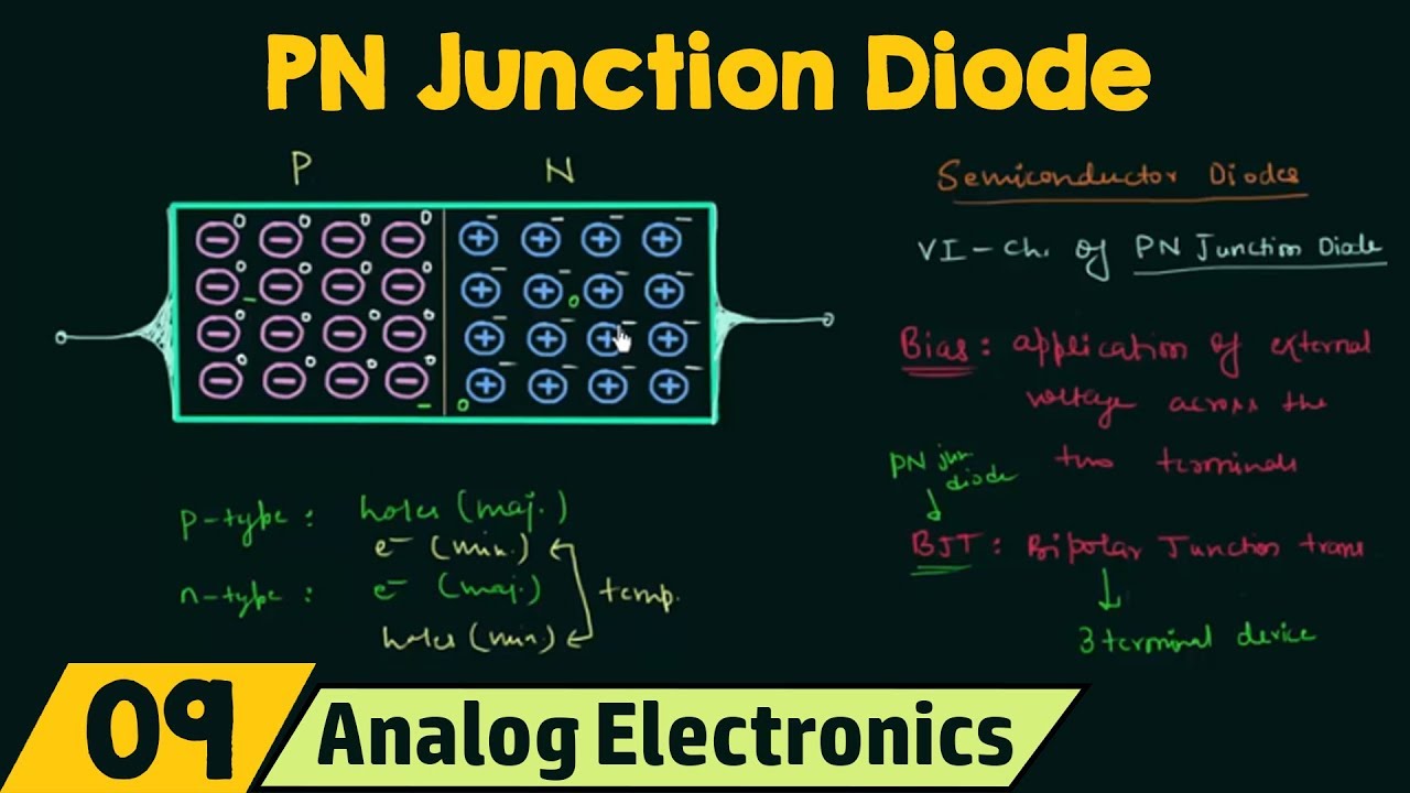
How does a P-N Junction Diode works? Explained through Animation
Summary
TLDRThis video explains the working of a diode in forward bias condition. It covers the structure of a diode made of P-type and N-type semiconductors, forming a P-N junction. When a diode is forward-biased, the external voltage reduces the potential barrier, allowing electrons and holes to cross the junction and create a current flow. The video also discusses the depletion region, forward voltage drop (0.7V for silicon diodes), and the low resistance in forward bias, ensuring minimal opposition to current. It concludes by introducing the concept of reverse bias, which will be explained in the next video.
Takeaways
- 😀 A P-type semiconductor consists of a large number of holes and few thermally generated electrons, with holes being the majority charge carriers.
- 😀 An N-type semiconductor consists of a large number of electrons and few thermally generated holes, with electrons being the majority charge carriers.
- 😀 When a P-type and N-type semiconductor are joined, a P-N junction is formed, creating a diode.
- 😀 The P-type terminal is called the anode, and the N-type terminal is called the cathode.
- 😀 The P-N junction creates a potential gradient due to the separation of charges (holes and electrons) across the junction.
- 😀 The diffusion process begins when electrons from the N-region are attracted towards the P-region, leaving behind immobile positive ions, while holes from the P-region diffuse into the N-region, leaving behind immobile negative ions.
- 😀 The diffusion of charge carriers eventually creates a depletion region, where no further diffusion of electrons or holes can occur.
- 😀 In forward bias condition, the negative terminal of the external source pushes electrons toward the P-side, while the positive terminal pushes holes towards the N-side.
- 😀 As the external voltage increases, more electrons and holes travel towards the junction, reducing the width of the depletion region and allowing current to flow.
- 😀 The forward voltage drop for a silicon diode is typically 0.7V, while for a germanium diode, it is 0.3V.
- 😀 The forward resistance of a diode is small (typically between 10 to 100 ohms), leading to a small voltage drop across the diode when conducting current.
Q & A
What are the majority charge carriers in P-type and N-type semiconductors?
-In P-type semiconductors, holes are the majority charge carriers, while in N-type semiconductors, electrons are the majority charge carriers.
How is a P-N junction formed?
-A P-N junction is formed when a P-type semiconductor and an N-type semiconductor are joined together using a specific fabrication technique.
What are the metallic terminals of the P-N junction called?
-The metallic terminal connected to the P-type material is called the anode, while the terminal connected to the N-type material is called the cathode.
What happens at the junction of a P-N semiconductor?
-At the junction, there is a high concentration of holes (positive charge) on the P-side and a high concentration of electrons (negative charge) on the N-side. This creates a potential gradient and initiates the diffusion process.
What is the process of diffusion in a P-N junction?
-In diffusion, electrons from the N-region move toward the P-region and combine with holes, leaving behind positive immobile ions. Similarly, holes from the P-region diffuse into the N-region, leaving behind negative immobile ions.
What happens when the depletion region of a P-N junction forms?
-The depletion region forms when a significant number of immobile ions accumulate near the junction, and the diffusion process slows down and eventually stops due to the opposing electric field created by these ions.
What is the effect of applying forward voltage to a diode?
-When a forward voltage is applied, the negative terminal of the external source pushes electrons towards the P-side, while the positive terminal pushes holes from the P-side to the N-side, reducing the width of the depletion region and allowing current to flow.
How does the depletion region region react to the forward voltage?
-As the forward voltage increases, more electrons and holes combine with ions in the depletion region, neutralizing them and reducing the potential barrier, allowing current to flow freely.
What is the forward resistance of a diode?
-The forward resistance of a diode is very small, typically between 10 to 100 ohms, which results in a small voltage drop across the diode when current flows in the forward direction.
What is the forward voltage drop of a silicon and a germanium diode?
-The forward voltage drop for a silicon diode is typically 0.7 volts, while for a germanium diode, it is around 0.3 volts.
Outlines

This section is available to paid users only. Please upgrade to access this part.
Upgrade NowMindmap

This section is available to paid users only. Please upgrade to access this part.
Upgrade NowKeywords

This section is available to paid users only. Please upgrade to access this part.
Upgrade NowHighlights

This section is available to paid users only. Please upgrade to access this part.
Upgrade NowTranscripts

This section is available to paid users only. Please upgrade to access this part.
Upgrade NowBrowse More Related Video

Cara Kerja Dioda PN Junction | Kuliah Fisika Semikonduktor

Simple Diode Circuit Calculations 1. Ideal Diode

Persambungan Semikonduktor PN pada Dioda | Kuliah Fisika Semikonduktor

EL DIODO. CIRCUITOS DE POLARIZACION DIRECTA E INVERSA.

Basic Electronics: PN Junction Working Principle and V-I Characteristics of PN Junction Diode

PN Junction Diode (No Applied Bias)
5.0 / 5 (0 votes)