Lecture 24 (CHE 323) CVD, part 1
Summary
TLDRThis lecture introduces chemical vapor deposition (CVD), a process used in semiconductor manufacturing for depositing materials like dielectrics, silicon, and metals. It contrasts CVD with physical vapor deposition, emphasizing the role of chemical reactions on the wafer surface. The lecture discusses the importance of heterogeneous reactions, the two-step mechanism of CVD involving gas diffusion and surface reaction, and the factors influencing deposition rate. It also explains the difference between diffusion-controlled and reaction-controlled regimes, highlighting how temperature affects these processes.
Takeaways
- 🌐 Chemical Vapor Deposition (CVD) is a process where chemical reactions create a film on a wafer surface.
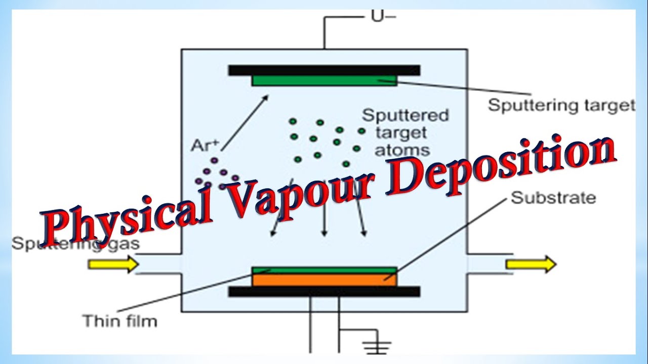
- 🔬 CVD is distinct from Physical Vapor Deposition as it involves chemical reactions for material creation.
- 🏭 CVD is used in semiconductor manufacturing to deposit dielectrics, silicon, and some metals like tungsten and titanium.
- 🔥 CVD is often performed in furnaces, which can be single wafer reactors or batch processing setups.
- 📉 The trend in the semiconductor industry is moving from batch to single wafer processing for better flexibility and control.
- 🧪 The film in CVD is created by reactions occurring on the wafer surface, which is a heterogeneous reaction.
- 📚 A simplified two-step mechanism for CVD involves gas phase reactants diffusing to the wafer surface and reacting there.
- 🔄 The rate of CVD can be limited by either the surface reaction or mass transport (diffusion), leading to different deposition regimes.
- 🌡️ Temperature significantly affects the deposition rate, with high temperatures favoring the diffusion-controlled regime.
- ⚖️ Maintaining a low partial pressure of reactants is crucial to prevent homogeneous gas phase reactions that can cause defects.
- 📈 Deposition rates are generally higher in the diffusion-controlled regime compared to the reaction-controlled regime.
Q & A
What is the main difference between chemical vapor deposition (CVD) and physical vapor deposition (PVD)?
-The main difference is that CVD involves chemical reactions to create the material being deposited, whereas PVD does not involve chemistry in the film creation process.
Why is heterogeneous CVD preferred over homogeneous CVD?
-Heterogeneous CVD is preferred because the reactions occur on the wafer surface, leading to uniform deposition and fewer defects, whereas homogeneous CVD can result in poor uniformity, particles, and defects as reactions happen in the gas phase.
What are the two main steps in the simplified CVD process described in the lecture?
-The two main steps are: 1) Diffusion of reactants from the gas phase to the wafer surface, and 2) Surface reactions that deposit the film.
What does it mean when a CVD process is 'diffusion-controlled'?
-In a diffusion-controlled process, the surface reaction is much faster than the diffusion of reactants to the wafer surface, meaning the deposition rate is limited by how quickly reactants can be transported to the surface.
What does it mean when a CVD process is 'reaction-controlled'?
-In a reaction-controlled process, the diffusion of reactants is fast enough to supply the reaction, but the deposition rate is limited by how quickly the reaction occurs at the wafer surface.
How does temperature affect the deposition rate in CVD?
-At low temperatures, the deposition rate is reaction-limited, meaning it increases significantly with temperature. At high temperatures, the deposition rate becomes diffusion-limited and changes slowly with temperature.
Why is it important to keep the partial pressure of reactants low in CVD?
-Keeping the partial pressure low helps prevent homogeneous gas-phase reactions that produce particles, which can lead to defects on the wafer surface.
What role does the mass transport coefficient (H_G) play in CVD?
-The mass transport coefficient (H_G) controls the rate of diffusion of reactants to the wafer surface. It influences whether the process is diffusion-limited or reaction-limited.
Why is achieving a high deposition rate important in CVD?
-High deposition rates are important because they improve manufacturing throughput, reduce the need for more equipment, and shorten cycle times in semiconductor production.
What is the relationship between activation energy and the different regimes in CVD?
-The surface reaction has a much higher activation energy than diffusion. At low temperatures, where activation energy dominates, the process is reaction-controlled. At higher temperatures, diffusion becomes the limiting factor as the reaction rate constant grows much faster with temperature than the mass transport coefficient.
Outlines

Esta sección está disponible solo para usuarios con suscripción. Por favor, mejora tu plan para acceder a esta parte.
Mejorar ahoraMindmap

Esta sección está disponible solo para usuarios con suscripción. Por favor, mejora tu plan para acceder a esta parte.
Mejorar ahoraKeywords

Esta sección está disponible solo para usuarios con suscripción. Por favor, mejora tu plan para acceder a esta parte.
Mejorar ahoraHighlights

Esta sección está disponible solo para usuarios con suscripción. Por favor, mejora tu plan para acceder a esta parte.
Mejorar ahoraTranscripts

Esta sección está disponible solo para usuarios con suscripción. Por favor, mejora tu plan para acceder a esta parte.
Mejorar ahora5.0 / 5 (0 votes)


