Chemical Vapor Deposition: Basic Function - Nanotechnology: A Maker’s Course
Summary
TLDRThis video explains Chemical Vapor Deposition (CVD), a key nanofabrication technique used to deposit thin films onto substrates. CVD is vital in producing materials with unique properties, like electrical conductivity or hydrophobicity, essential for advanced technologies such as microelectronics, solar panels, and LEDs. The process involves pumping gases into a vacuum chamber where they react and form thin films on substrates. Unlike Physical Vapor Deposition (PVD), CVD allows for more conformal coating, especially on complex surfaces. Various CVD methods, such as Plasma-Enhanced and Atomic Layer CVD, offer flexibility in material creation and application, making it central to industries like semiconductors and electronics.
Takeaways
- 😀 Chemical Vapor Deposition (CVD) is a key nanofabrication technique used to deposit thin films onto a substrate.
- 😀 Vapor deposition processes are carried out in a vacuum to prevent contamination from the external environment.
- 😀 There are two types of vapor deposition: Physical Vapor Deposition (PVD) and Chemical Vapor Deposition (CVD), with CVD involving gases instead of solid or liquid sources.
- 😀 Thin films deposited through CVD can enhance material properties, such as electrical, barrier, and physical properties.
- 😀 CVD allows for the creation of materials with specific applications, such as microelectronics, coatings for protection, and materials resistant to physical wear.
- 😀 CVD processes offer multi-directional deposition, allowing for uniform coating on complex surfaces, unlike PVD which may result in non-conformal films.
- 😀 Key factors that influence CVD include pressure, temperature, and plasma, as well as variations like plasma-enhanced and photoinitiated CVD.
- 😀 The deposition process in CVD is affected by various variables like reactor pressure, temperature, and the use of different stimulus forms such as plasma or UV light.
- 😀 Different CVD processes are categorized by their pressure conditions, such as atmospheric pressure, low pressure, and ultra-high vacuum.
- 😀 CVD is widely used in industries such as semiconductors, solar panels, LEDs, and integrated circuits for electronic devices, as well as in making protective coatings for materials.
Q & A
What is Chemical Vapor Deposition (CVD)?
-Chemical Vapor Deposition (CVD) is a nanofabrication technique used to deposit thin layers of material onto a substrate, such as glass or silicon, by introducing vaporized gases into a vacuum chamber where they react and form a thin film on the substrate.
Why must CVD processes be carried out in a vacuum chamber?
-CVD processes require a vacuum chamber to isolate the system from external atmospheric conditions and contaminants, ensuring the purity and consistency of the thin films being deposited.
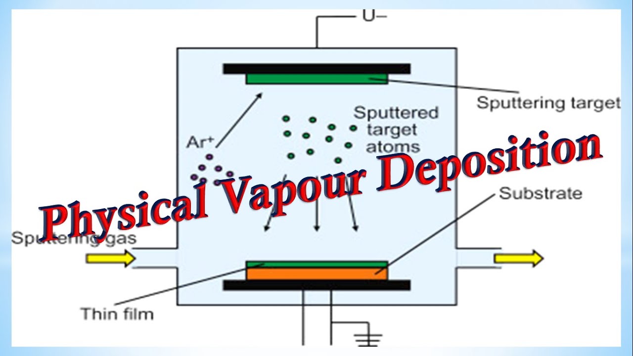
What is the main difference between Physical Vapor Deposition (PVD) and Chemical Vapor Deposition (CVD)?
-The main difference is in how the vapors are generated. In PVD, vapors are formed from solid or liquid materials through physical processes, while in CVD, gases are introduced in vapor form and react within the chamber to deposit thin films.
How does CVD achieve conformal deposition on complex surfaces?
-CVD achieves conformal deposition by allowing vapors to deposit in multiple directions, which ensures a smooth, uniform coating even on complex, geometrically challenging surfaces, such as trenches or rounded shapes.
What are some of the key properties that thin films deposited by CVD can possess?
-Thin films deposited by CVD can have various properties such as unique electrical conductivity, hydrophobicity, resistance to physical wear, or the ability to act as protective coatings against corrosion and rust.
What external stimuli can be used in CVD to initiate the reaction?
-External stimuli like heat, plasma, or UV light can be used to initiate or propagate the chemical reactions in CVD processes, depending on the specific material being deposited and the application.
Why is plasma-enhanced CVD used instead of traditional CVD?
-Plasma-enhanced CVD is used when materials, such as polymers or biological materials, would degrade at high temperatures. Plasma allows for a more controlled deposition process at lower temperatures.
What is Atomic Layer Deposition (ALD) in the context of CVD?
-Atomic Layer Deposition (ALD) is a variation of CVD where precursor gases are introduced one at a time, in a precise sequence, to allow for the deposition of extremely thin, controlled layers of material.
What industries benefit from CVD technology?
-Industries such as semiconductors, electronics, energy, and materials science benefit from CVD technology. It is used in the production of semiconductors, solar panels, LEDs, and advanced materials for various applications.
How is CVD used to improve material durability?
-CVD is used to create protective coatings that improve the durability of materials, such as making metals resistant to rust, corrosion, and wear, extending the lifespan of products.
Outlines

This section is available to paid users only. Please upgrade to access this part.
Upgrade NowMindmap

This section is available to paid users only. Please upgrade to access this part.
Upgrade NowKeywords

This section is available to paid users only. Please upgrade to access this part.
Upgrade NowHighlights

This section is available to paid users only. Please upgrade to access this part.
Upgrade NowTranscripts

This section is available to paid users only. Please upgrade to access this part.
Upgrade Now


5.0 / 5 (0 votes)