Merancang dan Membuat Single/ Double Layer PCB secara Manual dengan Metode Eksposure
Summary
TLDRThis educational video guides viewers through the manual process of designing and fabricating a Printed Circuit Board (PCB) using the Iron Transfer method. It covers all steps, from preparing the schematic design, printing the layout, and transferring it to the PCB, to etching, drilling, and finishing the board. The video emphasizes the importance of each stage in ensuring the quality and functionality of the PCB, providing a detailed yet easy-to-follow tutorial for electronics students and enthusiasts.
Takeaways
- 😀 The tutorial focuses on designing and fabricating a manual PCB using the Iron Transfer method, which is essential for electronics product development.
- 😀 The process begins with preparing and verifying the circuit schematic to ensure accuracy before moving to the PCB design.
- 😀 A PCB layout is designed using PCB design software on a computer, and the correct board size and component placement are crucial for a successful layout.
- 😀 The PCB layout is printed onto transfer paper using a LaserJet printer, with the image mirrored for correct alignment during the transfer process.
- 😀 The PCB is cleaned with fine sandpaper and water to prepare it for the toner transfer, ensuring the surface is smooth for better adhesion.
- 😀 The printed transfer paper is placed on the PCB, and an iron is used to press it firmly, transferring the toner design to the copper board.
- 😀 After transferring, the paper is removed by soaking the PCB in water and gently rubbing off the paper, leaving the toner image on the PCB.
- 😀 The etching process involves preparing a ferric chloride solution and immersing the PCB in it to dissolve the unprotected copper, leaving only the circuit traces.
- 😀 Once etching is complete, the PCB is cleaned with a wire brush, rinsed with water, and dried to remove any residues.
- 😀 The drilling process involves marking and drilling holes for the components, ensuring the holes are sized correctly and uniformly drilled.
- 😀 Silver nitrate is applied to the PCB to protect the copper traces, followed by cleaning and drying to finalize the board before assembly.
- 😀 A final protective clear coating is sprayed on the PCB to make the circuit traces more visible and protect them from corrosion or damage.
Q & A
What is the purpose of designing and creating a PCB manually in this lesson?
-The lesson aims to teach students how to manually design and create a printed circuit board (PCB), which is an essential skill in electronics for assembling various electronic components without using wires, based on a schematic diagram.
What is the importance of the PCB in electronics product manufacturing?
-The PCB is crucial in electronics because it connects various electronic components through conductive pathways, enabling the functionality of electronic devices. It provides a reliable and organized way to integrate different components into a circuit.
What is the first step in the process of creating a PCB?
-The first step is to prepare and verify the circuit schematic to ensure that it matches the desired design. This is done using appropriate software on a computer.
What is the role of layout design in PCB creation?
-The layout design is the process of determining the physical arrangement of components and their connections on the PCB. It is critical to ensure that the design matches the schematic and functions as intended.
What type of printer is used to print the PCB layout on transfer paper?
-A LaserJet printer is used to print the PCB layout onto transfer paper, as it produces a toner-based image that can be transferred onto the PCB surface.
Why is it necessary to clean the PCB with fine sandpaper and running water?
-Cleaning the PCB with fine sandpaper and running water removes any surface impurities and prepares the PCB for the transfer process, ensuring better adhesion of the toner and improving the quality of the PCB design.
How is the transfer of the PCB layout from paper to the PCB surface achieved?
-The layout is transferred by placing the printed transfer paper on the PCB and applying heat using an iron or press. The toner from the paper adheres to the PCB, creating the desired circuit pattern.
What is the purpose of the etching process in PCB creation?
-The etching process removes the excess copper from the PCB, leaving behind only the copper pathways that form the electrical connections between components. This is achieved by submerging the PCB in a chemical solution.
What chemicals are used in the etching process, and how should they be handled?
-The etching process uses a solution made of 150 mL of water, 200 mL of sodium hydroxide (NaOH), and 50 mL of hydrochloric acid (HCl). Proper care should be taken when handling these chemicals, including wearing protective gear and working in a well-ventilated area.
What should be done after the etching process to finalize the PCB?
-After etching, the PCB should be cleaned, dried, and inspected to ensure that all unwanted copper has been removed. A final layer of protective clear coat may be applied to preserve the design, and the PCB should be checked for any issues before moving to the next steps.
Outlines

此内容仅限付费用户访问。 请升级后访问。
立即升级Mindmap

此内容仅限付费用户访问。 请升级后访问。
立即升级Keywords

此内容仅限付费用户访问。 请升级后访问。
立即升级Highlights

此内容仅限付费用户访问。 请升级后访问。
立即升级Transcripts

此内容仅限付费用户访问。 请升级后访问。
立即升级浏览更多相关视频
How to Make an Automatic Emergency Light || Power Failure Backup Light
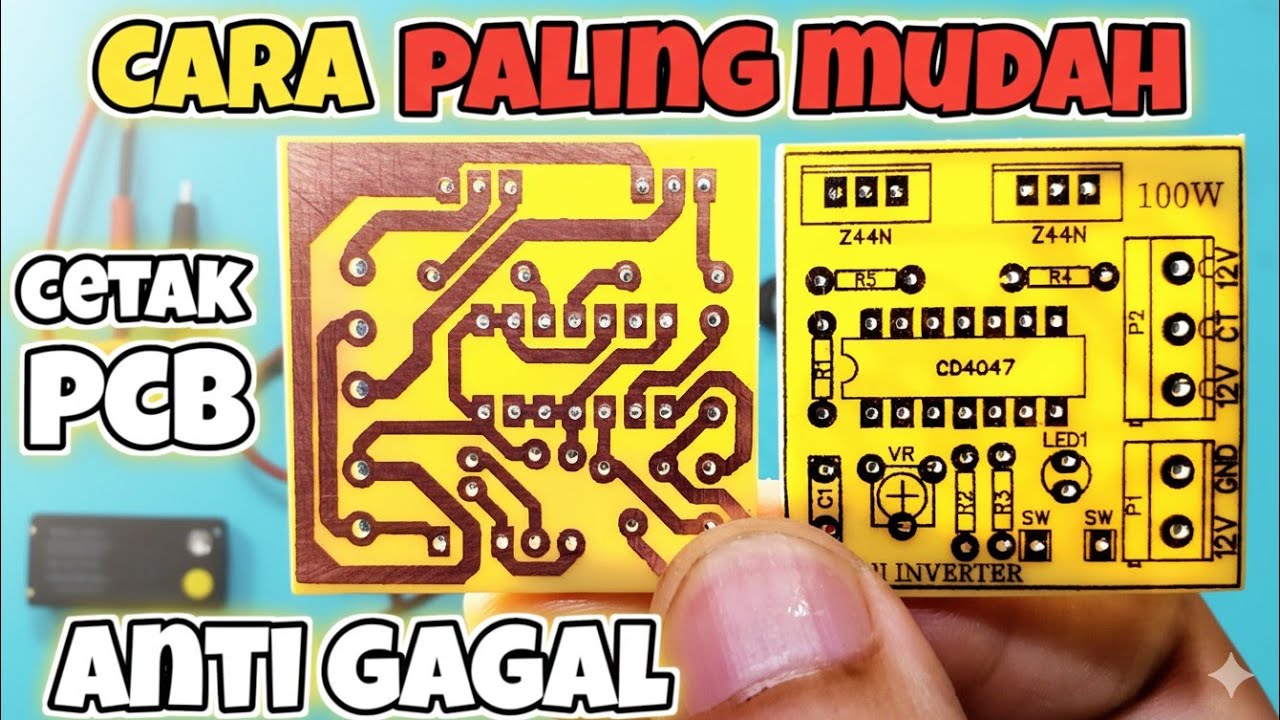
CARA CETAK PCB MANUAL Paling mudah anti gagal

Kicad Beginner Tutorial- A Traffic Light for Arduino ( RE-UPLOADED, Twice )

IoT Based Plant Watering System Indoor project using ESP32 Blynk | IoT Projects 2023
pH meter Arduino, pH Meter Calibration, DIYMORE pH Sensor, pH Sensor Arduino Code, pH of liquids

I made a Kirby Diorama!
5.0 / 5 (0 votes)
