Introduction to Scanning Electron Microscopy (SEM)

Penn State MRI
24 Dec 202104:08

Summary

TLDRWes Auker, a Research Technologist at Penn State, provides an introduction to Scanning Electron Microscopy (SEM). SEM uses a focused electron beam to gather data on sample morphology, chemical composition, and crystalline structure. The technique generates 2D images and is useful for surface morphology, elemental contrast, and chemical composition analysis. Applications include EDS for composition analysis and EBSD for crystal orientation. SEM is valued for its rapid results, ease of use, and ability to analyze from macro to nanostructures, though it has limitations in surface analysis compared to other techniques like Auger Spectroscopy.

Takeaways

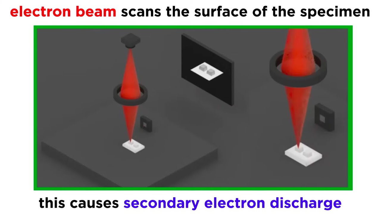
  • 🔬 Scanning Electron Microscopy (SEM) uses a focused beam of high-energy electrons to generate signals from a solid specimen's surface.
  • 📏 SEM reveals critical information about a sample, including its morphology, chemical composition, and crystalline structure.
  • 🖼️ SEM generates 2D images that display spatial variations in surface properties based on electron interactions.
  • ⚛️ SEM can perform qualitative and quantitative compositional analysis using EDS (Energy Dispersive Spectroscopy) and crystalline analysis using EBSD (Electron Backscatter Diffraction).
  • 💡 The interaction volume of SEM varies depending on the accelerating voltage and materials, extending from under 100 nanometers to 5 microns into the surface.
  • 🌀 Low-energy secondary electrons, ejected from conduction or valence bands, are commonly used for imaging in SEM.
  • 📊 SEM applications include surface morphology, elemental contrast, phase structure analysis, and chemical composition mapping.
  • 📈 Back-scattered electron imaging in SEM helps identify materials by atomic number, with brighter features indicating higher atomic numbers.
  • ⚙️ SEM offers advantages like fast results, flexibility in sample sizes, and ease of user training but is not a true surface technique compared to Auger Spectroscopy or XPS.
  • 🚀 Technical specifications include sub-nanometer resolution, an interaction volume range from 50 nanometers to 5 microns, and gun voltage from 250V to 30kV.

Q & A

  • What is the primary function of a Scanning Electron Microscope (SEM)?

    -A Scanning Electron Microscope (SEM) uses a focused beam of high-energy electrons to generate signals at the surface of solid specimens. These signals reveal information about the sample, including its morphology, chemical composition, crystalline structure, and orientation.

  • What types of information can SEM imaging provide about a sample?

    -SEM imaging provides information on surface morphology, chemical composition, crystalline structure, and crystal orientations of materials that make up the sample.

  • How are 2-dimensional images generated in SEM analysis?

    -In most SEM applications, data are collected over a selected area of the sample's surface, and 2-dimensional images are generated that display spatial variations in the properties of the sample.

  • What are some specialized analysis techniques used in SEM?

    -Specialized SEM techniques include Energy Dispersive X-ray Spectroscopy (EDS) for chemical composition analysis, and Electron Backscatter Diffraction (EBSD) for determining crystalline structure and crystal orientations.

  • What is the 'interaction volume' in the context of SEM?

    -The 'interaction volume' refers to the region where primary electron beams interact with the sample, losing energy through random scattering and absorption. This volume extends from less than 100 nanometers up to 5 microns into the sample surface, depending on factors like accelerating voltage and material.

  • What is the significance of secondary electrons in SEM imaging?

    -Secondary electrons, which have low energy (less than 50 eV), are commonly used for imaging in SEM. These electrons are ejected from the sample's conduction or valence bands through inelastic scattering with beam electrons and originate from just a few nanometers below the sample surface.

  • What are some common applications of SEM?

    -Common SEM applications include surface morphology, elemental contrast, chemical composition analysis, phase structure analysis, fracture analysis, surface contamination studies, semiconductor inspection, and grain structure analysis.

  • How do backscattered electron images differ from secondary electron images?

    -Backscattered electron images are based on the atomic number of the scanned material. Higher atomic numbers produce brighter features, while lower atomic numbers result in darker features in the image.

  • What are some advantages of using SEM?

    -Advantages of SEM include fast results for analyzing various sample sizes (from small powders to large wafers), ease of user training, and the ability to analyze materials at macro, micro, and nanoscales.

  • What are some disadvantages of SEM compared to other surface techniques?

    -Compared to techniques like Auger Spectroscopy or X-ray Photoelectron Spectroscopy (XPS), SEM is not a true surface technique because the interaction volume extends beyond the surface, typically greater than 10 nanometers. Additionally, SEM often requires dry samples and may need standards for quantitative analysis.

Outlines

00:00

🔬 Introduction to Scanning Electron Microscopy (SEM)

Wes Auker, a Research Technologist at Penn State University, introduces the basics of Scanning Electron Microscopy (SEM). SEM uses a focused beam of high-energy electrons to generate signals that provide detailed information about a specimen's surface, including morphology, chemical composition, and crystalline structure. The technique is commonly applied to generate 2D images, revealing spatial variations of the material properties. SEM also performs qualitative and quantitative compositional analysis using techniques such as Energy Dispersive Spectroscopy (EDS) and Electron Backscatter Diffraction (EBSD).

📊 Interaction Volume and SEM Imaging Techniques

The paragraph explains how the electron beam interacts with the sample, losing energy through scattering and absorption within the ‘interaction volume,’ which can vary based on the accelerating voltage and materials analyzed. A secondary electron image of cellulose fibers demonstrates SEM's capabilities. SEM commonly collects low-energy secondary electrons from near the sample’s surface, allowing detailed surface analysis. These electrons come from conduction or valence bands of the sample's atoms, allowing SEM to create high-resolution images of material surfaces.

🔍 SEM Applications and Imaging Techniques

This section lists key applications of SEM, such as surface morphology, elemental contrast, and chemical composition analysis, among others. It highlights examples of EDS mapping, showing images unrelated to each other but used for illustration. It explains that backscatter electron images, which depend on the atomic number of the materials scanned, are common in SEM. Higher atomic numbers produce brighter features, while lower numbers result in darker features.

⚡ Advantages and Limitations of SEM

SEM offers advantages such as fast results, the ability to analyze various sample sizes, and ease of use. SEM can also analyze materials from the macro to nano scale. However, it is not a true surface technique due to the interaction volume being greater than 10 nanometers, and dry samples are preferred in high vacuum modes. The paragraph mentions common SEM applications like EDS, EBSD, and semiconductor fault isolation.

📈 Technical Specifications of SEM

This section details the technical specifications of contemporary SEMs, including sub-nanometer resolution, interaction volumes ranging from 50 nanometers to 5 microns, and gun voltage ranges between 250 volts and 30 kilovolts. It also mentions that evacuation times in SEMs typically take less than five minutes, emphasizing the efficiency and capabilities of modern SEM technologies.

Mindmap

Keywords

💡Scanning Electron Microscope (SEM)

A scanning electron microscope (SEM) is a powerful tool that uses a focused beam of high-energy electrons to analyze the surface of solid specimens. It generates various signals that provide information about the sample's morphology, chemical composition, and crystalline structure. SEM is central to the video's theme, serving as the core technology for the analysis techniques discussed.

💡Interaction Volume

The interaction volume is the teardrop-shaped region within a sample where electrons from the SEM interact with the material, causing scattering and absorption. It extends from less than 100 nanometers to several microns below the surface. This concept is key to understanding how SEM works and why it may not be suitable for analyzing extremely thin surface layers.

💡Secondary Electrons

Secondary electrons are low-energy electrons (less than 50 eV) ejected from a material’s atoms due to interactions with the electron beam. These electrons originate from just a few nanometers below the surface and are commonly used to create detailed 2D images of the sample's morphology. The video highlights their importance in surface imaging.

💡Back-scattered Electrons

Back-scattered electrons are high-energy electrons that are reflected back from the sample after interaction with the electron beam. These electrons are sensitive to the atomic number of the material, making them useful for differentiating between elements in a sample. In the video, they are mentioned in the context of material analysis, particularly for identifying atomic contrast.

💡Energy Dispersive Spectroscopy (EDS)

EDS is a technique used in SEM to perform chemical composition analysis by detecting X-rays emitted from the sample as a result of electron interactions. It provides qualitative and quantitative information about the elements present in a specific area. EDS is one of the core applications of SEM, as highlighted in the video.

💡Electron Backscatter Diffraction (EBSD)

EBSD is a technique used in SEM to analyze crystalline structure and orientation by measuring the pattern of diffracted electrons. It is particularly useful for characterizing grain structures and boundaries in materials. The video mentions EBSD as a complementary technique to EDS for structural analysis.

💡Morphology

Morphology refers to the study of the shape, structure, and texture of a sample's surface. In SEM, morphology can be visualized by collecting secondary electron signals, which give detailed 2D images of surface features. The video discusses how SEM provides crucial insights into the morphology of materials like cellulose fibers and minerals.

💡Accelerating Voltage

Accelerating voltage is the energy level of the electron beam used in SEM. It determines the depth of penetration into the sample, influencing the size of the interaction volume. Higher voltages allow deeper analysis, while lower voltages are better for surface detail. The video mentions this in the context of controlling the depth of electron interactions.

💡Surface Contamination

Surface contamination refers to unwanted materials or particles on the sample's surface that can interfere with SEM imaging and analysis. In the video, surface contamination is listed as one of the potential issues SEM can help identify during surface inspections. Clean, dry samples are typically required for high-quality results.

💡Resolution

Resolution in SEM refers to the microscope's ability to distinguish between two close points on a sample. Modern field-emission SEMs can achieve sub-nanometer resolution, allowing for highly detailed imaging of micro- and nanostructures. This is one of the technical specifications discussed in the video, emphasizing SEM’s capability for high-precision analysis.

Highlights

Introduction to Scanning Electron Microscopy (SEM) and its basic principles.

SEM uses a focused beam of high-energy electrons to generate signals at the surface of solid specimens.

SEM provides detailed information about morphology, chemical composition, and crystalline structure.

SEM generates 2D images showing spatial variations in the properties of the sample.

SEM can perform both qualitative and quantitative compositional analysis using EDS and EBSD techniques.

Explanation of the 'Interaction Volume,' a teardrop-shaped volume where electron scattering and absorption occur.

SEM commonly captures low-energy secondary electrons, which are ejected from the specimen’s conduction or valance bands.

Applications of SEM include surface morphology, elemental contrast, phase structure, fracture analysis, and more.

Examples of EDS mapping and corresponding composition maps.

Back-scattered electron imaging is dependent on the atomic number of scanned materials, where higher atomic numbers result in brighter features.

SEM's advantages include fast results, usability across a variety of sample sizes, and the ability to capture details from macro to nanostructures.

SEM's limitations include its non-surface-specific nature and the requirement for dry samples in high-vacuum modes.

Standard Interaction Volume ranges from 50 nanometers to 5 microns, depending on the analysis.

Common technical specifications include sub-nanometer resolution, voltage range from 250 volts to 30 KV, and short evacuation times.

Conclusion summarizing SEM's capabilities in surface morphology, EDS, EBSD, and semiconductor fault isolation.

Transcripts

play00:01

Hello, my name is Wes Auker, I'm a Research Technologist with

play00:05

Materials Characterization Lab at Penn State University and I'm

play00:09

going to be walking you through an Introduction to Scanning

play00:12

Electron Microscopy (SEM).  A scanning electron microscope uses a

play00:15

focused beam of high energy electrons to generate a variety

play00:19

of signals at the surface of solid specimens. The signals that are

play00:23

generated from electrons sample interaction, reveal information

play00:25

about the sample including morphology, chemical composition,

play00:28

and crystalline structure and orientation of materials making

play00:31

up the sample.

play00:33

In most applications, data are collected over a selected area

play00:36

of the surface of the sample and 2-dimensional images generated

play00:40

that display spatial variations

play00:41

in these properties.  The SEM is also capable of performing

play00:46

qualitative and quantitative compositional analysis of

play00:48

selected regions on the sample, and this approach is especially

play00:52

useful in determining chemical compositions using EDS,

play00:55

crystalline structure and crystal orientations using EBSD.

play00:59

The diagram on the left here, shows an interaction volume.  When the

play01:03

primary electron beam interacts with the sample, the electrons

play01:06

lose energy by repeated random scattering and absorption within

play01:10

a teardrop shape volume of the specimen, known as the

play01:13

Interaction Volume, which extends from less than 100 nanometers to

play01:17

anywhere up to five microns into the surface, depending on the

play01:21

accelerating voltage and the materials under analysis.  And then

play01:24

on the right here, we have a secondary electron image of interwoven

play01:27

cellulose fibers. The most common imaging modes,

play01:30

collect low energy, less than 50 EV secondary electrons, that

play01:34

are ejected from Conduction or Valance Bands of the specimen

play01:37

atoms by inelastic scattering interactions with

play01:39

beam electrons.  Due to their low energy, these electrons

play01:42

originate from within a few nanometers below the sample

play01:46

surface.

play01:47

Some applications of SEM are: Surface Morphology, Elemental

play01:52

Contrast, Chemical Composition, Phase Structure,

play01:55

Fracture Analysis, Surface Contamination, Semiconductor

play01:58

Inspection, Voltage Contrast Imaging, Grain Structures &

play02:02

Boundaries, X-Ray analysis done through EDS, and Diffraction

play02:07

Analysis done through EBSD.

play02:10

Just some examples here of some basic EDS mapping. These images

play02:16

aren't related to one another.

play02:18

Just here as examples.  Here on the left, we have a secondary

play02:22

electron image of a mineralogical surface and then

play02:25

the corresponding composition map and spectrum.  And on the

play02:29

right, we have a back-scattered electron image of battery

play02:32

material on carbon felt.  And back-scatter images are pretty

play02:35

common, an SEMs and are dependent on the atomic number of the scanned

play02:39

materials. The higher this value, the brighter the feature on the

play02:43

image.  And the lower the atomic number value, the darker the

play02:48

feature will appear in the image.

play02:51

Some advantages of SEM, depending on the number of

play02:55

samples you have, typically have pretty fast results.  A variety

play02:59

of sample sizes, from small amounts of powder to a full six-inch

play03:04

wafer, ease of user trainability, and anywhere from

play03:08

macro to micro structure to nanostructure materials.

play03:11

Disadvantages relative to something like Auger Spectroscopy

play03:14

or XPS, it's not a true surface technique. The interaction

play03:19

volume is typically greater than

play03:21

10 nanometers. Quantitative analysis does require standards.

play03:25

Dry samples are usually pretty much the standard in high

play03:31

vacuum modes with field emission SEMs. some applications:  Surface

play03:36

Morphology, Elemental Contrast, EDS, EBSD, and

play03:39

Semiconductor Fault Isolation.  Some general technical specs:

play03:44

Sub-nanometer resolution. It's pretty common with contemporary

play03:48

field emission SEMs.

play03:51

Standard Interaction Volume: Anywhere from 50 nanometers to

play03:54

five microns. A Gun Voltage Range:  Anywhere from 250 volts

play03:58

all the way to 30 KV.  And most Evacuation Times are less than

play04:03

five minutes. Thank you very much.

Rate This

5.0 / 5 (0 votes)

相关标签
SEM basicsElectron MicroscopyMaterial AnalysisEDSEBSDImaging TechniquesSurface MorphologyChemical CompositionMicroscopy ApplicationsNanostructure
您是否需要英文摘要?