Introduction to Registers | What is Shift Register? Types of Shift Registers

ALL ABOUT ELECTRONICS
17 Sept 202210:54

Summary

TLDRThis video from the All About Electronics YouTube channel dives into the concept of registers in digital circuits, focusing on their role as memory elements capable of storing multiple bits of data. It explains the basic 4-bit register, its limitations, and how it can be improved with a load signal to control data input without occupying the data bus continuously. The video also introduces shift registers, discussing their ability to shift binary data between connected flip flops and the various methods of data loading and retrieval. The potential applications of shift registers in time delay generation, data conversion, and arithmetic operations are highlighted, with a promise of more detailed exploration in future videos.

Takeaways

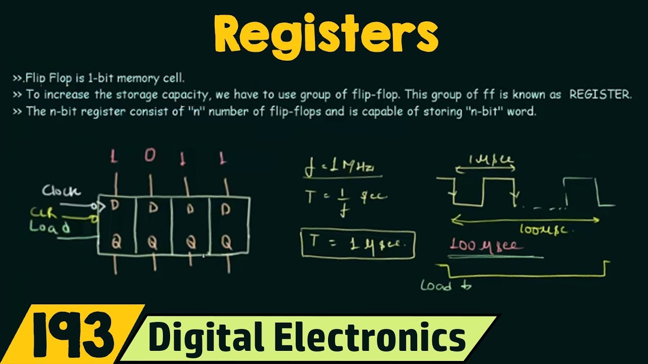
  • 😀 Registers are groups of flip flops that can store n-bit data in digital circuits.
  • 🔁 D flip flops are commonly used in registers due to their single input and straightforward data storage at clock transitions.
  • ⏰ The basic function of a register is to store data at each clock transition and make it accessible at the output.
  • 🚫 A plain register is impractical as it continuously occupies the data bus, which can be problematic in synchronous systems.
  • 🔄 An AND gate can be used to control the clock signal to a register, enabling data loading only when required.
  • 🛑 The load signal in a register acts as a synchronous input, loading data at clock transitions when high.
  • 🔧 Registers can be equipped with an asynchronous clear input to reset all flip flops to zero when activated.
  • 🔄 Shift registers are a type of register where binary data can be shifted between neighboring flip flops.
  • 🔢 Shift registers can be loaded and retrieved in two ways: serially or in parallel, leading to four types based on these combinations.
  • 🕒 Shift registers are useful not only for data storage but also for time delay generation, data conversion, and arithmetic operations.
  • 📚 The video promises to cover more details on different types of shift registers in upcoming videos.

Q & A

  • What is the basic function of a flip flop in digital circuits?

    -A flip flop is a basic memory element in digital circuits that can store only one bit of information.

  • Why are multiple flip flops needed in a digital circuit like a microprocessor?

    -Multiple flip flops are needed to store or process data in multiple bits, such as 16, 32, or 64 bits, as these circuits handle more complex data storage and processing.

  • What is a register in the context of digital circuits?

    -A register is a group of flip flops that can store n bits of data, allowing for the storage of larger data sets in a single unit.

  • Why are D flip flops typically used in registers?

    -D flip flops are used in registers because they have only one input, which simplifies the process of storing the input data at the clock transition.

  • How does the presence of a Master Clock affect the operation of a register?

    -The Master Clock, being common between different digital blocks, dictates the timing of data storage in a register. If the register operates at 1 gigahertz, data at the inputs is loaded into the register every nanosecond.

  • What is the issue with using a register without any control mechanism for data loading?

    -Without a control mechanism, the register would continuously load data from the data bus, potentially occupying it for an extended period and preventing other components from accessing it.

  • How can the data bus be freed up by controlling the register's clock?

    -By enabling the clock only when data needs to be loaded into the register through an AND gate controlled by a load signal, the data bus can be used more efficiently and not occupied continuously.

  • What is the drawback of using an AND gate to control the clock signal in a synchronous system?

    -Using an AND gate introduces a propagation delay, causing the register to receive the clock signal after a delay, which is undesirable in synchronous systems where all elements should receive the clock simultaneously.

  • How does a load signal control the operation of a register?

    -A load signal, when high, allows data bits to reach the flip flops through an AND gate and be loaded into the register at the clock transition. When the load signal is low, the register maintains the previous data.

  • What is a shift register and how does it differ from a standard register?

    -A shift register is a type of register where the output of one flip flop is connected to the input of the next, allowing for the shifting of binary data between neighboring flip flops, which is not present in a standard register.

  • What are the two methods of loading data into a shift register?

    -The two methods of loading data into a shift register are serial loading, where new bits are loaded with each clock pulse, and parallel loading, where all bits are loaded simultaneously in a single clock cycle.

  • What are the four types of shift registers based on data loading and retrieval methods?

    -The four types of shift registers are serial IN serial OUT, serial IN parallel OUT, parallel IN serial OUT, and parallel IN parallel OUT, each determined by the method of data loading and retrieval.

  • What additional applications can shift registers be used for beyond data storage?

    -Shift registers can be used for time delay generation, serial to parallel conversion, parallel to serial data conversion, and arithmetic operations.

Outlines

00:00

📚 Introduction to Registers and Shift Registers

The first paragraph introduces the concept of registers in digital circuits, emphasizing their role as memory elements capable of storing multiple bits of data, unlike flip flops which store only one bit. It explains that registers are groups of flip flops sharing a common clock and typically use D flip flops due to their single input feature. The paragraph also discusses practical issues with using registers, such as data bus occupation and the introduction of a load signal to control data loading, which avoids constant data bus usage. The importance of synchronous operation in digital systems and the avoidance of controlling the clock signal are also highlighted.

05:03

🔄 Understanding Load Control and Shift Registers

This paragraph delves into the mechanism of load signals in registers, illustrating how data bits are controlled and loaded into the register upon a high load signal during a clock transition. It explains the process of maintaining previous data when the load signal is low, facilitated by the feedback from the flip flop's output to its input. The paragraph also introduces shift registers, which differ from standard registers by allowing binary data to be shifted between neighboring flip flops. It outlines the two methods of data loading in shift registers: serial and parallel, and the two methods of data retrieval: serial out and parallel out. The summary also mentions the four types of shift registers based on these loading and retrieval methods.

10:08

🛠️ Applications and Future Discussion on Shift Registers

The final paragraph highlights the diverse applications of shift registers beyond mere data storage, such as time delay generation, serial to parallel data conversion, and arithmetic operations. It sets the stage for upcoming videos that will explore different types of shift registers in more detail. The paragraph concludes with an invitation for viewers to engage with the content by asking questions, offering suggestions, and subscribing to the channel for further educational content.

Mindmap

Keywords

💡Registers

Registers are a group of flip flops that can store n bits of data in digital circuits. They are essential for handling multiple bits of information, such as in microprocessors or microcontrollers, which process data in larger bit sizes like 16, 32, or 64 bits. The script mentions that registers are composed of D flip flops, which are convenient for this purpose due to their single input and straightforward data storage mechanism at clock transitions. An example from the script is a 4-bit register, where each bit is stored in a separate flip flop that shares a common clock.

💡Flip Flops

Flip flops are basic memory elements in digital circuits that can store a single bit of information. They are the building blocks of registers, as mentioned in the script, where multiple flip flops are used to store multiple bits of data. The D flip flop, in particular, is highlighted as a common choice for registers due to its simple input structure. The script explains that whatever input is applied to a D flip flop, it will be stored upon the clock transition.

💡Shift Registers

Shift registers are a type of register that allows the shifting of binary data between neighboring flip flops. They are used for various purposes, including time delay generation, serial to parallel conversion, and arithmetic operations. The script describes two methods of data loading into a shift register: serial and parallel. Additionally, it outlines two methods for data retrieval: serial out and parallel out, leading to four types of shift registers based on these combinations.

💡D Flip Flop

The D flip flop is a specific type of flip flop used in registers due to its single data input, labeled 'D' for 'data'. It is mentioned in the script as the memory element typically used in registers because the data presented at its input during a clock transition is exactly what gets stored. This feature makes D flip flops ideal for constructing registers that need to capture and hold data bits.

💡Clock Transition

A clock transition refers to the change in the state of a clock signal, which is a fundamental aspect of synchronous digital circuits. In the context of the script, the clock transition is the moment at which the data present at the inputs of flip flops in a register is stored. This concept is crucial for understanding how data is captured and updated in registers and shift registers.

💡Load Signal

The load signal is a control input in a register that, when high, enables the loading of data into the register at the next clock transition. The script explains that this signal can be used to control when data is loaded, thus avoiding the need to occupy the data bus continuously. The load signal is synchronous, meaning it only affects the register in conjunction with the clock signal.

💡Data Bus

A data bus is a collection of signals used to transmit data within a system. In the script, it is mentioned that in a typical synchronous digital system, registers need to ensure data stability on the data bus for a certain duration, such as 300 microseconds, to load data accurately. The data bus is an essential component for data transfer between different parts of a digital system.

💡Propagation Delay

Propagation delay refers to the time it takes for a signal to travel through a circuit or system. The script discusses the implications of propagation delay in the context of using an AND gate to control the clock signal to a register. This delay can cause the register to receive the clock signal later than the master clock, which is undesirable in synchronous systems that require simultaneous clock reception by all elements.

💡Clear Input

The clear input is an asynchronous control signal used in registers and other digital circuits to reset the circuit to a known state, typically zero. In the script, it is described as active low, meaning that when the clear input is low, all flip flops in the register are reset. This feature is important for initializing registers before new data is loaded.

💡Synchronous Digital Systems

Synchronous digital systems are circuits where the operation of digital elements is synchronized by a common clock signal. The script emphasizes the importance of all synchronous elements receiving the clock signal at the same time, which is why controlling the clock signal, as in the case of the load signal and AND gate, is generally avoided in such systems.

💡Serial and Parallel Data Loading

Serial data loading involves loading data bit by bit over multiple clock cycles, while parallel data loading allows all bits to be loaded simultaneously in a single clock cycle. The script explains these concepts in the context of shift registers, which can be loaded either serially through a single input or parallelly through multiple accessible inputs.

Highlights

Introduction to registers in digital circuits and their importance as basic memory elements.

Explanation of how flip-flops, as basic memory elements, can store only one bit of information.

Description of registers as a group of flip-flops capable of storing n-bit data.

Diagram of an n-bit register with each flip-flop sharing a common clock.

Use of D flip-flops in registers due to their single input and convenience for data storage.

Functioning of a basic 4-bit register with individual inputs and outputs for each flip-flop.

Challenges of using registers with a common Master Clock in synchronous digital systems.

The concept of data bus occupation and its impact on system performance.

Solution to control data loading into registers using a load signal and an AND gate.

Avoidance of controlling the clock signal in synchronous systems due to propagation delay issues.

Control of register operation by managing data inputs instead of the clock signal.

Introduction of load and clear inputs in registers for data loading and resetting.

Explanation of shift registers and their ability to shift binary data between neighboring flip-flops.

Two methods of data loading in shift registers: serial and parallel.

Two methods of data retrieval from shift registers: serial out and parallel out.

Four types of shift registers based on data loading and retrieval methods.

Practical applications of shift registers in time delay generation, data conversion, and arithmetic operations.

Upcoming detailed exploration of different types of shift registers in future videos.

Invitation for questions, suggestions, and engagement through likes and subscriptions.

Transcripts

play00:06

Hey, friends welcome to the YouTube channel  ALL ABOUT ELECTRONICS. So in this video,  

play00:12

we will learn about the registers in the digital  circuits. And at the later part of the video,  

play00:18

we will also talk about the shift registers. So,  so far we have seen the different types of flip  

play00:24

flops. And we understood that, this flip flops are  very basic memory element in the digital circuits.  

play00:31

And we have also seen that, this flip flop  can store only one bit of information.  

play00:36

But if you take any digital circuit, for  example a microprocessor or the microcontroller,  

play00:41

then it stores or process the data in the  multiple bits. Like 16 bits, 32 bits or 64 bits.  

play00:49

So if you want to store this data,  then we require multiple flip flops.  

play00:54

So this group of flip flops, which can store  the n bit of data are called the registers.  

play01:00

So this is the diagram of the n bit register. And  here, each flip flop is sharing the common clock.  

play01:08

So if the n is equal to 4, then we will have the  4 bit register. So this is the very basic type  

play01:14

of 4 bit register. Now typically in the register,  the D flip flops are used as the memory element.  

play01:21

Because as you know, this D flip flop has only one  input. And in the D flip flop, whatever input we  

play01:28

apply at the input side, the same will be stored  in the flip flop at the clock transition. And  

play01:34

therefore, it is convenient to use the D flip flop  in the registers. So here this B1 B2 B3 and B4 are  

play01:42

the inputs of this register. And as you can see,  each input is connected to the individual input  

play01:48

of the flip flop. So at the clock transition,  whatever input is present at these four inputs,  

play01:54

the same will be stored in the register at the  clock transition. That means this is the very  

play01:59

basic type of register, which can store the data  at the every clock transition. And if you want to  

play02:05

access that data, then that can be also accessed  at the output side. But practically, this register  

play02:12

is of no use. So let me explain why? Now typically  if you see any synchronous digital system, then  

play02:19

it has the Master Clock, which is common between  the different digital blocks. So let's say, this  

play02:25

register is also getting the common Master Clock.  And let's say it is operating at the 1 gigahertz.  

play02:33

That means the duration of the clock is equal  to 1 nanosecond. So we can say that, at every 1  

play02:40

nanosecond, whatever data is present at these four  inputs, the same will be loaded into the register.  

play02:46

So let's say, we have some data, which we  want to store for the 300 microseconds.  

play02:52

So here we also need to make sure that,  these four inputs, or the inputs of the data  

play02:58

bus it's not changing up to 300 microsecond.  Because if the data changes before that time,  

play03:03

then whatever random input is present at the  data bus that will be stored in the register.  

play03:09

That means we need to ensure that, the data is  available on the data bus up to 300 microsecond.  

play03:15

So in a way, here we are also occupying  this data bus up to 300 microseconds.  

play03:21

And in between, if any other register in the  system, wants to access this data bus, then it  

play03:27

won't be able to access that data bus. So let's  see, what we can do to avoid all these issues. So  

play03:33

the one solution is, we can just enable the clock  whenever we want to load the data in the register.  

play03:40

So for that, we can apply this clock  to the resistor through this AND gate.  

play03:45

So whenever this load signal is high, then only  this clock will be delivered to the register.  

play03:51

And whatever data is present at the inputs,  the same will be loaded into the register.  

play03:57

So whenever this load signal will become low,  then this clock will also get disabled. And  

play04:02

as you know, whenever there is a no clock pulse,  then the flip flop will retain its current state.  

play04:08

So in this way, whatever data which is loaded  into the register, it will remain as it is.  

play04:14

And once again it will change,  whenever this load signal is high.  

play04:18

So in this way, we are not occupying  the data bus over the entire time.  

play04:23

But generally this approach is not preferred.  And typically anything which controls the clock  

play04:29

signal, is usually avoid in the synchronous  digital systems. Because here, due to this AND gate, 

play04:36

this register will receive the clock after  the certain propagation delay. That means there  

play04:41

is a propagation delay, between the Master Clock  and the clock which is received by the register.  

play04:47

And in the synchronous systems, it is preferred  that, all the synchronous elements receive the  

play04:51

clock at the same time. That means, this approach  is typically avoided in the synchronous systems.  

play04:58

So rather controlling the clock signal, the  operation of the register is controlled by the  

play05:03

controlling the data inputs. So this is how, the  data bits are controlled using the load signal.  

play05:10

So as you can see, whenever this load signal is  high, then the data bits B1 B2 B3 and B4 will  

play05:17

reach to the flip flop, through this AND gate.  And at the clock transition, that data will be  

play05:22

loaded into the register. Now whenever this load  signal is high, then this load bar will become  

play05:28

low. And therefore, the output of the second  AND gate will become 0. That means in that case,  

play05:34

the second AND gate will remain disabled. Now  whenever, this load signal will become low,  

play05:40

then the output of this first AND gate will become  0. But now, since the load bar will become high,  

play05:47

so this input will become high. And now whatever  output is present at the output of the flip flop,  

play05:54

the same will be given back to the input.  And in this way, the flip flop will hold its  

play06:00

current data. That means whenever, you just want  to load the new data, then first of all make the  

play06:06

data available on this data bus. And then after  just enable this load signal. And when this load  

play06:13

signal is low, then the register will maintain the  previous data. So this is the very basic register  

play06:19

with the load input. And here, this load signal is  the synchronous input. Meaning that once this load  

play06:26

signal is high, then the data will be get loaded  into the register, only at the clock transition.  

play06:32

So along with the load signal, we can  also have the asynchronous clear input.  

play06:37

So here as you can see, this clear input  is the active low. That means whenever  

play06:42

this clear input is low, then all the flip  flops in the register will get reset to zero.  

play06:48

So if we represent the same circuit in the block  diagram, that this is how it can be represented.  

play06:54

So here, this B1 to B4 are the inputs,  while the Q1 to Q4 are the outputs.  

play07:00

And apart from that, we have also this load signal  and the clear input. So in this type of register,  

play07:07

we can store the data, or we can retrieve the  data. But there is another type of register, where  

play07:13

it is possible to shift the binary data, between  the neighboring flip flops of the register.  

play07:18

So this type of register is known as the shift  register. So in this type of register, the output  

play07:25

of the one flip flop is connected to the input  of the next flip flop. So if you see the register  

play07:31

circuit, we have discussed so far, in that there  is a no interconnection between the flip flops.  

play07:37

But in the shift register, the neighboring  flip flops are the interconnected.  

play07:42

So in the shift register, there are two ways  the data can be loaded. The one is the serially.  

play07:49

That means at the every clock pulse, the new bit  will get loaded into the register. So if we have a  

play07:55

4 bit register, then in the four clock pulses, the  data will get loaded into the register. So in this  

play08:02

type of register, the register has only one input.  Now the second method of loading is the parallel  

play08:09

load. So in the parallel load, all the bits of  the register, will get loaded in the single clock.  

play08:16

So if we have a 4 bit shift register, then for the  parallel load, this 4 input should be accessible.  

play08:23

And by applying the inputs to these four lines,  the new data can be loaded into the register  

play08:27

in the single clock. That means, there are two  possible ways, to load the data into the register.  

play08:34

Similarly, there are two ways to retrieve  the data from the shift register.  

play08:39

And the one is the serial out. So in the serial  out, we have only one output line. And at every  

play08:47

clock, we can access only, one output bit. So in a  4 bit shift register, to retrieve the data of the  

play08:53

register, you will require 4 clock signals. Now  the second method is the parallel out. So in this  

play09:01

parallel out, we can access all the output bits  in The single clock. So if we have a 4 bit shift  

play09:07

register, then for the parallel out, all the four  outputs of the flip flop should be accessible.  

play09:13

So depending on, how the data is loaded into the  shift register, and how the data is retrieved,  

play09:18

we have total four types of shift registers. That  is serial IN, serial OUT. serial IN parallel OUT,  

play09:25

parallel IN serial OUT, and parallel IN  parallel OUT. So in the first type of  

play09:31

register, the data is serially loaded into the  register, and it is also taken out serially.  

play09:37

Then in this serial IN parallel OUT type of  shift register the data is loaded serially,  

play09:42

but it can be accessed parallelly. Then in this  parallel IN serial OUT type of shift register,  

play09:49

the data is loaded parallelly, but it  can be taken out serially. And likewise,  

play09:55

in this parallel IN parallel OUT type of shift  register the data is loaded parallelly, and it  

play10:01

is also taken out parallelly. So this is similar  to the register, which we have discussed earlier.  

play10:08

So these are the four types of shift registers.  So apart from the storage, because of its shifting  

play10:14

property, these shift registers are also useful in  many other applications. Like for the time delay  

play10:20

generation, and serial to parallel conversion.  Apart from that, they can also be used for the  

play10:25

parallel to serial data conversion, as  well as in the arithmetic operations.  

play10:30

So in the upcoming videos, we will learn in detail  about this different types of shift registers. But  

play10:36

I hope in this video, you got the basic idea  about the register, and this shift register.  

play10:41

So if you have any question or suggestion, then  do let me know here in the comment section below.  

play10:46

If you like this video, hit the like button, and  subscribe to the channel for more such videos.

Rate This

5.0 / 5 (0 votes)

Related Tags
Digital CircuitsRegistersShift RegistersFlip FlopsMemory ElementsData StorageElectronics TutorialSynchronous SystemsLoad SignalClear Input