CARA MEMBUAT LAYOUT PCB SECARA MANUAL
Summary
TLDRThis video offers a detailed guide on manually designing a PCB, highlighting the importance of creative freedom and technical precision. It walks through the key steps, such as component placement, routing traces, and grounding, while stressing the significance of following the schematic for accurate connections. The video also emphasizes minimizing the size of the PCB for efficiency, all while ensuring neatness during soldering. It encourages experimenting with layout designs, but always prioritizes correct functionality and careful connections to ensure a successful PCB creation process.
Takeaways
- 😀 Transistor connection types, such as base-collector-emitter, should be carefully considered when designing a PCB layout.
- 😀 Creativity plays a significant role in PCB design; different designers can produce varying layouts from the same schematic.
- 😀 It's essential to follow the correct component arrangement, particularly when positioning transistors on the PCB.
- 😀 Pay close attention to the component's largest physical size when deciding the initial placement on the PCB.
- 😀 Ensure all electrical connections are precise, and components are correctly aligned to prevent errors in the circuit.
- 😀 The order of placing components on the PCB doesn't need to follow a fixed rule, but large components often go first.
- 😀 Use the correct placement for the ground and power connections to avoid short circuits or incorrect wiring.
- 😀 The base of a transistor can be connected to different circuit points based on the design's requirements.
- 😀 Avoid crossing ground and positive voltage paths on the PCB to ensure proper operation of the circuit.
- 😀 The final layout should be compact and efficient, with fewer traces and a neat design to improve the circuit's performance.
- 😀 Adding labels and clear markings on the PCB helps in troubleshooting and maintaining a clean, understandable layout.
Q & A
What is the primary focus of the script?
-The script primarily focuses on manually designing and creating a Printed Circuit Board (PCB), particularly with transistors and other components like resistors.
Why is creativity emphasized in the PCB design process?
-Creativity is emphasized because the layout and design of a PCB can vary depending on individual preferences and approaches. The key is ensuring the connections are accurate and follow the provided schematic.
How do you decide where to start when designing the PCB layout?
-The layout usually starts with placing the largest component first, as it typically influences the positioning of other parts. In the example, the transistor is placed first due to its size.
What is the importance of transistor footings in the PCB design?
-The transistor footings (such as base, collector, and emitter) must be positioned correctly according to the schematic. The placement of these footings impacts the overall functionality of the circuit.
What should be considered when designing the PCB for a specific transistor?
-When designing the PCB, it is important to refer to the schematic of the chosen transistor, especially the pin configuration (base, collector, emitter), and ensure the layout reflects this accurately.
What is the function of the resistors in the circuit described in the script?
-Resistors, such as the R22k, are used to limit current flow and ensure proper operation of the transistor in the circuit. The specific resistors mentioned help connect various parts of the circuit to manage the signal flow.
What role does grounding play in the PCB design?
-Grounding is crucial as it ensures the circuit operates safely by providing a common reference point for all components. In the design, ground connections are made by linking parts like the emitter of the transistor to the ground plane.
How is the PCB layout for this project different from other designs?
-This PCB layout might differ in terms of the size and placement of components. The script suggests that different designers may have varying layouts, and the design can be optimized to make the circuit more compact and efficient.
What is the purpose of using a schematic in the PCB design process?
-A schematic provides a blueprint for the circuit. It helps the designer understand how components are connected and guides the placement and routing of connections in the PCB layout.
Why is the speaker making a specific point about the layout being 'neat' or 'not cluttered'?
-The speaker emphasizes that a clean and organized layout is crucial for the clarity and functionality of the PCB. While some components can be labeled for clarity, the overall design should remain clean to ensure better readability and performance.
Outlines

This section is available to paid users only. Please upgrade to access this part.
Upgrade NowMindmap

This section is available to paid users only. Please upgrade to access this part.
Upgrade NowKeywords

This section is available to paid users only. Please upgrade to access this part.
Upgrade NowHighlights

This section is available to paid users only. Please upgrade to access this part.
Upgrade NowTranscripts

This section is available to paid users only. Please upgrade to access this part.
Upgrade NowBrowse More Related Video
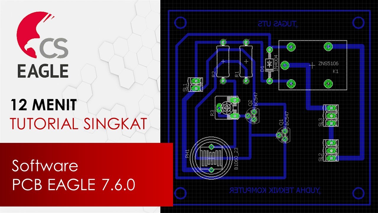
12 Menit Tutorial Desain PCB Eagle 7.6.0

Merancang dan Membuat Single/ Double Layer PCB secara Manual dengan Metode Eksposure

PCB Challenges for 5–6 GHz Radar Design

How does Inverter work? What are the Main Components of Inverter & Their Working in Hindi?

Significant Figures and Measurement

Paganini Technique for Beginners 17 : How to practice a piece : Küchler op.11 - Technical Mastery
5.0 / 5 (0 votes)