Varactor (Construction & Working) Special Purpose Diode (Basic Electronics) BE/BTech 1st year
Summary
TLDRThis lecture dives into the principles of semiconductor physics, specifically focusing on the behavior of PN junction diodes and their capacitance. The content explains how the capacitance of a diode varies with changes in input voltage and the width of the depletion layer. The relationship between reverse voltage, depletion layer expansion, and capacitance reduction is explored in detail. The practical application of variable capacitors in electronic devices is highlighted, with the emphasis on how changes in voltage affect the diode's behavior. This foundational knowledge is key for students in electronics and semiconductor design.
Takeaways
- 😀 The topic of the video is focused on semiconductors, particularly on how changes in the depletion layer affect capacitance.
- 😀 The behavior of a PN junction diode and how its depletion layer interacts with voltage changes is explored.
- 😀 A key concept introduced is the relationship between input voltage changes and the resulting changes in capacitance in semiconductor devices.
- 😀 The video explains that when input voltage increases, the capacitance of the device varies, which is characteristic of a variable capacitor.
- 😀 The depletion layer in a semiconductor device expands or contracts based on the applied reverse voltage, which in turn influences the capacitance.
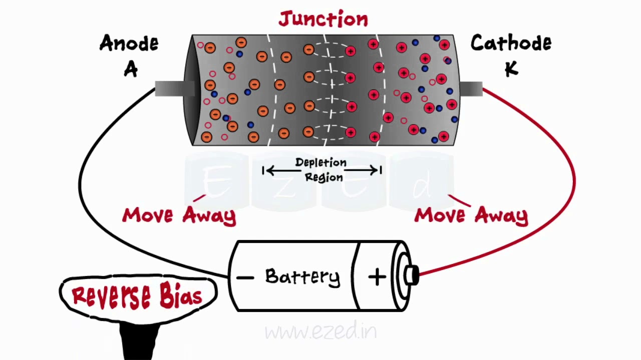
- 😀 The behavior of a reverse-biased diode in a PN junction is demonstrated, showing how the depletion layer changes with reverse voltage.
- 😀 As the reverse voltage increases, the depletion layer grows, reducing the overall capacitance between the two terminals.
- 😀 The video emphasizes the importance of the relationship between voltage and depletion layer changes, which directly impacts the capacitor's functionality.
- 😀 A visual representation of the changes in capacitance and depletion layer is shown using a graph, illustrating the effects of reverse voltage on capacitance.
- 😀 The practical application of variable capacitors in electronic circuits is introduced, with a focus on their use in specific student electronics exams.
Q & A
What is a PN junction diode, and how does it function?
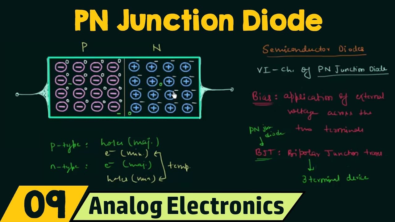
-A PN junction diode consists of two regions: the P-type (positive) and N-type (negative) semiconductors. When they come into contact, electrons from the N-type region recombine with holes from the P-type region, creating a depletion layer. This layer prevents further flow of charge carriers, and the diode only allows current to flow in one direction when forward biased, or blocks current when reverse biased.
What is the significance of the depletion layer in a PN junction diode?
-The depletion layer is the region where electrons and holes recombine, resulting in a lack of charge carriers. This region acts as a barrier to the flow of current. When a reverse voltage is applied, the depletion layer widens, and this behavior influences the diode's capacitance, which is key in understanding how the diode responds to varying electrical conditions.
How does reverse voltage affect the depletion layer and capacitance of a PN junction diode?
-As reverse voltage increases, the depletion layer widens, reducing the capacitance. Initially, at lower reverse voltages, the capacitance is higher, but as the reverse voltage increases, the electric field strengthens, pushing charge carriers away, causing the depletion region to grow and capacitance to decrease.
Why is the relationship between reverse voltage and capacitance important in semiconductor devices?
-This relationship is important because it allows for the design of devices such as **variable capacitors**, which change capacitance in response to an applied reverse voltage. This principle is applied in circuits like **tuning circuits**, **voltage-controlled oscillators**, and **signal modulators**, where the capacitance needs to vary with voltage.
What role does the electric field play in the behavior of a PN junction diode?
-The electric field in the depletion region of a PN junction diode is responsible for the direction of current flow. It also plays a crucial role in determining the width of the depletion region. As reverse voltage is increased, the electric field becomes stronger, pushing more charge carriers out of the region and widening the depletion layer.
What is the difference between the depletion region and the capacitance in a reverse-biased PN junction?
-In a reverse-biased PN junction, the depletion region grows as reverse voltage increases, which reduces the capacitance. The capacitance is inversely related to the width of the depletion layer. As the depletion region widens, it creates a smaller effective area for charge storage, resulting in lower capacitance.
How does the reverse potential affect the characteristics of the depletion region and the capacitance?
-As reverse potential increases, the depletion region expands, leading to an increase in the electric field. This causes the capacitance to decrease because the wider depletion region provides less charge storage capability. The relationship between reverse voltage and capacitance is crucial in tuning semiconductor devices in applications requiring variable capacitance.
What is meant by the term 'variable capacitor' in semiconductor electronics?
-A **variable capacitor** refers to a capacitor whose capacitance can be adjusted or varied by changing an external condition, such as reverse voltage applied to a PN junction diode. This allows for precise control of the capacitance, which is useful in circuits where tuning or frequency adjustment is required, such as in radio or signal processing devices.
What graphical representation was discussed to show the relationship between reverse potential and capacitance?
-The graph discussed shows how capacitance changes with reverse potential. As reverse potential increases, the capacitance initially decreases. At lower reverse potentials, the capacitance is higher, while at higher potentials, the depletion region widens, and the capacitance reaches a minimum. This graph helps visualize the impact of voltage changes on the diode's performance.
How do practical applications of PN junction diodes utilize these characteristics of capacitance?
-In practical applications, the characteristics of PN junction diodes—especially their variable capacitance—are utilized in circuits like **voltage-controlled oscillators**, **variable tuning circuits**, and **signal modulators**. These devices exploit the change in capacitance with reverse voltage to adjust frequency, filter signals, or modulate frequencies in communication systems.
Outlines

Этот раздел доступен только подписчикам платных тарифов. Пожалуйста, перейдите на платный тариф для доступа.
Перейти на платный тарифMindmap

Этот раздел доступен только подписчикам платных тарифов. Пожалуйста, перейдите на платный тариф для доступа.
Перейти на платный тарифKeywords

Этот раздел доступен только подписчикам платных тарифов. Пожалуйста, перейдите на платный тариф для доступа.
Перейти на платный тарифHighlights

Этот раздел доступен только подписчикам платных тарифов. Пожалуйста, перейдите на платный тариф для доступа.
Перейти на платный тарифTranscripts

Этот раздел доступен только подписчикам платных тарифов. Пожалуйста, перейдите на платный тариф для доступа.
Перейти на платный тарифПосмотреть больше похожих видео

Diodes - What Are Diodes - PN Junction - Forward Bias - Reverse Bias - Zener Diodes

PN Junction Diode (No Applied Bias)

Schottky Diode (Construction & Working) Special Purpose Diodes (Basics Electronics)

V-I Characteristics of PN Junction Diode in Hindi | TECH GURUKUL By Dinesh Arya

Lab 4 and 5: PN junctions and Solar Cells

Types of Diodes - The Learning Circuit
5.0 / 5 (0 votes)
