Implementation of all logic gates with NAND gate | Design with universal gates | digital electronics
Summary
TLDRIn this educational video from RF Design Basics, viewers learn how to implement all basic logic gates using only NAND gates. The tutorial covers designing NOT, AND, OR, XOR, and XNOR gates step by step, explaining the required configurations and underlying logic. Key concepts such as De Morgan's Law are introduced to simplify circuit analysis, while detailed explanations show how multiple NAND gates can replicate the behavior of other gates. By the end of the video, learners gain a clear understanding of how to construct complex logic functions using just one type of gate, enhancing their digital electronics skills.
Takeaways
- 😀 The lecture explains how to implement all basic logic gates using only NAND gates.
- 😀 A NOT gate can be created by connecting both inputs of a single NAND gate to the same input signal, producing an inverted output.
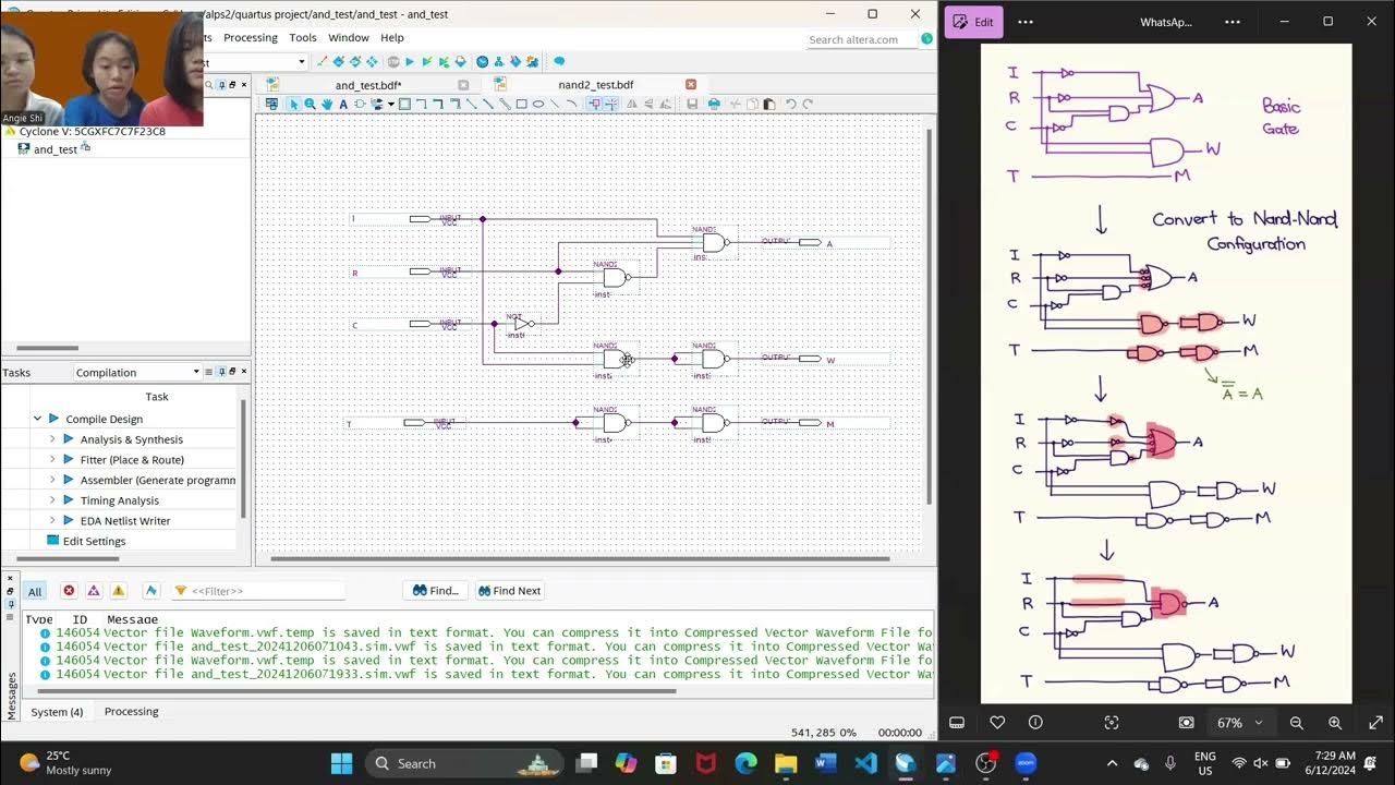
- 😀 An AND gate is designed by first taking a NAND of the inputs and then inverting the result using a NOT gate.
- 😀 An OR gate can be implemented using three NAND gates by first inverting each input and then applying a NAND operation on the inverted signals.
- 😀 De Morgan’s law is used to simplify NAND-based OR gate designs, where (A·B)̅ = A̅ + B̅ and (A + B)̅ = A̅·B̅.
- 😀 An XOR gate requires four NAND gates and produces a high output only when the inputs are different.
- 😀 The XOR gate design uses intermediate NAND outputs that are combined and simplified to achieve the correct logic function.
- 😀 An XNOR gate is created by taking the output of an XOR gate and passing it through a NAND-based NOT gate, producing a high output when inputs are the same.
- -
- 😀 NAND gates are universal, meaning all other logic gates (NOT, AND, OR, XOR, XNOR) can be derived from them.
- -
- 😀 The video demonstrates step-by-step methods and explanations for designing each logic gate using NAND gates, emphasizing both practical implementation and theoretical reasoning.
Q & A
What is the purpose of this video on RF Design Basics?
-The purpose of the video is to demonstrate how to implement various logic gates—NOT, AND, OR, XOR, and XNOR—using NAND gates.
How is a NOT gate implemented using a NAND gate?
-A NOT gate is implemented using a single NAND gate with both of its inputs connected to the same signal. This configuration produces the inverted output, or A bar (¬A).
What is the significance of using NAND gates to design other logic gates?
-Using NAND gates to design other logic gates is crucial because NAND gates are universal gates. This means any other logic gate can be constructed using only NAND gates, which simplifies circuit design and reduces component requirements.
How is an AND gate designed using NAND gates?
-An AND gate can be designed using a NAND gate followed by an inverter. The NAND gate's output is inverted to produce the AND operation (A AND B).
What role does De Morgan's law play in designing gates with NAND gates?
-De Morgan's law is used to transform expressions involving AND and OR operations into equivalent forms that can be realized with NAND gates. For example, an AND operation can be expressed as the NAND of the inputs' negations, and vice versa for OR operations.
How is an OR gate implemented with NAND gates?
-An OR gate is implemented using two NAND gates to invert the inputs, followed by a third NAND gate that combines the outputs. The final output corresponds to the OR operation between the two inputs.
How do you design an XOR gate using NAND gates?
-An XOR gate is designed using four NAND gates. Two inputs are fed into the first two NAND gates to create intermediate outputs, which are then combined using the third and fourth NAND gates to produce the XOR result.
What is the logic behind the design of an XOR gate using NAND gates?
-The XOR gate design uses the fact that XOR results in true when the inputs differ. By applying De Morgan's law and simplifying the intermediate expressions, the output from the four NAND gates gives the XOR logic (A XOR B).
What is the difference between XOR and XNOR gates in this design?
-The XOR gate outputs true when the inputs are different, while the XNOR gate is the negation of XOR, outputting true when the inputs are the same. The XNOR gate is designed by adding a NOT gate to the XOR gate's output.
How is an XNOR gate implemented using NAND gates?
-An XNOR gate is implemented by first designing the XOR gate using NAND gates and then adding a NOT gate to invert the XOR output. This results in the XNOR functionality, which outputs true when the inputs are equal.
Outlines

Cette section est réservée aux utilisateurs payants. Améliorez votre compte pour accéder à cette section.
Améliorer maintenantMindmap

Cette section est réservée aux utilisateurs payants. Améliorez votre compte pour accéder à cette section.
Améliorer maintenantKeywords

Cette section est réservée aux utilisateurs payants. Améliorez votre compte pour accéder à cette section.
Améliorer maintenantHighlights

Cette section est réservée aux utilisateurs payants. Améliorez votre compte pour accéder à cette section.
Améliorer maintenantTranscripts

Cette section est réservée aux utilisateurs payants. Améliorez votre compte pour accéder à cette section.
Améliorer maintenantVoir Plus de Vidéos Connexes

Implementation ( Realization ) of all logic gates using NAND gate and NOR gates | DLD | STLD | DE

Logic Gates | OR gate | AND gate | NOT gate | NOR gate | NAND gate | Digital Circuits (in हिन्दी)
Demonstration of combinational logic design using Quartus Prime software

Design of CMOS NAND gate

[Part 1] Unit 1.2 - Boolean Functions

Module 1.3: Basic Gates
5.0 / 5 (0 votes)
