VHDL code for 4 bit ALU and Realization on FPGA development Board
Summary
TLDRIn this instructional video, the presenter guides viewers through the process of designing a 4-bit ALU (Arithmetic Logic Unit) using VHDL code. The tutorial covers understanding ALU's logical functions and boolean expressions, creating an Xilinx ISE project, coding, simulating, synthesizing, and generating a bit file for FPGA implementation. The presenter also demonstrates how to create a UCF file for pin constraints and uses an FPGA programmer to load the ALU functionality onto the board, testing it with switches and LEDs to verify the operations.
Takeaways
- 😀 The video is a tutorial on designing a 4-bit ALU (Arithmetic Logic Unit) using VHDL and implementing it on an FPGA development board.
- 🔍 The presenter starts by explaining the logical functions and boolean expressions of the ALU before writing the VHDL code.
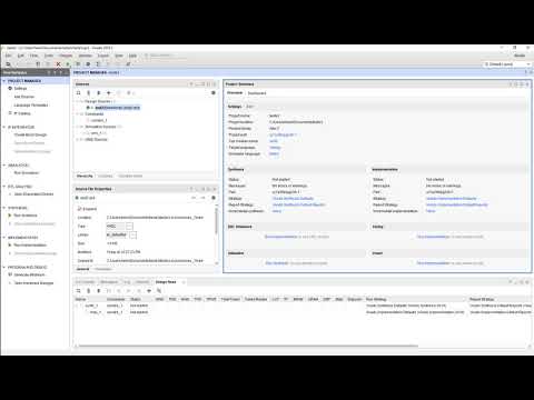
- 💻 The tutorial involves creating a project in Xilinx ISE, writing VHDL code for the 4-bit ALU, simulating the code, and synthesizing it.
- 📈 The ALU performs various operations based on the select line inputs, including addition, subtraction, AND, NAND, XOR, XNOR, OR, and passing through the input A.
- 🔢 The inputs to the ALU consist of two 4-bit inputs (A and B) and a 3-bit select line, with the output being a 4-bit ALU result.
- 📝 The VHDL code uses a 'with select' statement to handle different operations based on the select line values.
- 🔩 The synthesis process involves implementing the ALU using components like adders, subtractors, and multiplexers.
- 🖥️ The video demonstrates a simulation of the ALU to verify its functionality for different select line inputs and operations.
- 🔌 A UCF (User Constraint File) is created to define pin connections for the FPGA implementation, specifying the physical connections for inputs, outputs, and select lines.
- 💾 The final step involves generating a bit file, programming the FPGA board, and testing the ALU functionality using switches and LEDs on the board.
Q & A
What is the main topic of the video session?
-The main topic of the video session is to write VHDL code for a 4-bit ALU (Arithmetic Logic Unit) and its implementation on an FPGA development board.
What are the logical functions and boolean expressions needed to understand before writing the VHDL code for the ALU?
-Before writing the VHDL code, one must understand the logical functions such as addition, subtraction, AND, OR, XOR, and NAND operations, as well as the boolean expressions that represent these functions in the ALU design.
What is the purpose of the select line in the 4-bit ALU design?
-The select line in the 4-bit ALU design is used to choose between different operations such as addition, subtraction, AND, OR, XOR, and other functions based on the combination of bits set on the select line.
How many bits are in the select line for the 4-bit ALU design?
-The select line for the 4-bit ALU design is 3 bits, allowing for eight different combinations of operations.
What is the process of implementing the VHDL code on the FPGA development board?
-The process involves writing the VHDL code, creating a project in Xilinx ISE, simulating the code, synthesizing it, creating a UCF file, generating a bit file, and then implementing the bit file on the FPGA development board.
What is a UCF file used for in the context of FPGA implementation?
-A UCF (User Constraint File) is used to define pin connections between the FPGA and external components, specifying the physical pins to which the signals in the VHDL code are assigned.
How many different operations can be performed with the 4-bit ALU design as described in the script?
-With the 3-bit select line, the 4-bit ALU design can perform eight different operations, each corresponding to a unique combination of the select line bits.
What is the significance of the 'others' clause in the VHDL code for the ALU?
-The 'others' clause in the VHDL code for the ALU is used to handle any remaining cases that are not explicitly covered by the select statements, ensuring that all possible input combinations are accounted for.
What are the steps involved in testing the ALU functionality on the FPGA board?
-The steps include loading the bit file onto the FPGA, connecting the select lines and input switches to the appropriate pins on the FPGA, and observing the LED outputs to verify that the ALU performs the expected operations based on the selected operation.
How does the video script guide the user to verify the simulation of the ALU operations?
-The script guides the user to verify the simulation by providing examples of input values for A and B, and the expected results for each operation based on the select line settings. It also demonstrates how to force values in the simulation and observe the outputs to confirm the correctness of the ALU operations.
Outlines

Esta sección está disponible solo para usuarios con suscripción. Por favor, mejora tu plan para acceder a esta parte.
Mejorar ahoraMindmap

Esta sección está disponible solo para usuarios con suscripción. Por favor, mejora tu plan para acceder a esta parte.
Mejorar ahoraKeywords

Esta sección está disponible solo para usuarios con suscripción. Por favor, mejora tu plan para acceder a esta parte.
Mejorar ahoraHighlights

Esta sección está disponible solo para usuarios con suscripción. Por favor, mejora tu plan para acceder a esta parte.
Mejorar ahoraTranscripts

Esta sección está disponible solo para usuarios con suscripción. Por favor, mejora tu plan para acceder a esta parte.
Mejorar ahoraVer Más Videos Relacionados
5.0 / 5 (0 votes)


