Analisis transistor BJT : Prategangan DC dan Sinyal AC Kecil
Summary
TLDRThe video presentation focuses on analyzing a BJT transistor circuit. The presenters, Rehan Tertia Putra and Iryanti, walk through the process of determining key values like current (Ic, Ib), and calculating the transistor’s amplification using techniques like Thevenin’s Theorem and small-signal analysis. They present both DC and AC analysis methods, sharing calculations for parameters such as the base current (Ib), collector current (Ic), and gain. The analysis involves simulated data and real calculations, showing the behavior of the transistor in different conditions and the results of their tests and simulations.
Takeaways
- 😀 The presentation starts with an introduction by Rehan Tertia Putra and Iryanti, members of group 05 J, explaining their goal to present an analysis of a BJT transistor assignment.
- 😀 The circuit being discussed involves a DC biasing source with an AC non-active source and a capacitor in the circuit.
- 😀 The Thevenin's theorem is applied to simplify the circuit and calculate various resistances, including R2, which is 8.2 ohms, and using the formula for Thevenin's equivalent resistance.
- 😀 A detailed calculation of the Thevenin resistance (Rth) and the equivalent resistance is provided, which results in a value of 7.5 ohms.
- 😀 To calculate the base current (Ib), the formula involving Thevenin's resistance is applied, yielding a value of 0.015 mA.
- 😀 The current gain (Ic) of the transistor is computed using the beta value of 90 and the base current (Ib), giving an Ic of 1.305 mA.
- 😀 An AC small signal analysis is performed to calculate the transistor’s voltage gain, with Rp calculated as 1.73k ohms.
- 😀 The transconductance (gm) is determined using the formula involving the thermal voltage (26mV), resulting in a value of -0.051.
- 😀 The final small signal gain is calculated, providing an overall gain of -33.8.
- 😀 The presentation concludes with a discussion on the simulation results, where the measured values for Ic and Ib from the simulation match closely with the theoretical calculations.
Q & A
What was the main objective of the presentation?
-The main objective was to present the analysis of the BJT transistor, including both DC and AC small signal analysis, and to demonstrate how Thevenin's Theorem was applied to simplify the circuit for easier calculation.
What is Thevenin's Theorem and how was it applied in this analysis?
-Thevenin's Theorem simplifies complex circuits by replacing them with a single voltage source and resistance. In this analysis, it was used to calculate the Thevenin equivalent resistance and voltage, which were then used to calculate base and collector currents.
How was the Thevenin equivalent resistance calculated?
-The Thevenin equivalent resistance was calculated using the parallel combination of resistors R1 and R2, resulting in a value of 7.5 kΩ.
What is the significance of the base current (Ib) in the BJT transistor analysis?
-The base current (Ib) is crucial as it is used to calculate the collector current (Ic) using the transistor's current gain (β). It also plays a key role in determining the transistor’s operating point.
How was the collector current (Ic) calculated?
-The collector current (Ic) was calculated using the formula Ic = β * Ib, where β is the current gain of the transistor. With β = 90 and Ib = 0.015 mA, the collector current Ic was found to be approximately 1.3 mA.
What does the small signal analysis aim to achieve in this context?
-The small signal analysis is used to determine the transistor’s small signal parameters, such as the transconductance (gm) and voltage gain, which are essential for understanding the transistor’s behavior in response to small AC signals.
What is the formula for calculating transconductance (gm) in small signal analysis?
-The transconductance (gm) is calculated using the formula gm = Ic / Vt, where Vt is the thermal voltage (approximately 26 mV at room temperature).
What value was obtained for the transconductance (gm) in this analysis?
-The transconductance (gm) was calculated to be 0.05, based on the previously calculated Ic value of 1.3 mA.
How does the voltage gain of the transistor relate to the small signal parameters?
-The voltage gain is related to the small signal parameters, such as transconductance (gm) and the load resistance (Rp). It is calculated using the formula Voltage Gain = -gm * Rp, where the negative sign indicates an inverted signal.
What were the results of the simulation, and how did they compare to the theoretical calculations?
-The simulation results showed Ic ≈ 1.27 mA and Ib ≈ 14.6 µA, which closely matched the theoretical calculations of Ic ≈ 1.3 mA and Ib = 0.015 mA, indicating the accuracy of both the theoretical and simulated models.
Outlines

Esta sección está disponible solo para usuarios con suscripción. Por favor, mejora tu plan para acceder a esta parte.
Mejorar ahoraMindmap

Esta sección está disponible solo para usuarios con suscripción. Por favor, mejora tu plan para acceder a esta parte.
Mejorar ahoraKeywords

Esta sección está disponible solo para usuarios con suscripción. Por favor, mejora tu plan para acceder a esta parte.
Mejorar ahoraHighlights

Esta sección está disponible solo para usuarios con suscripción. Por favor, mejora tu plan para acceder a esta parte.
Mejorar ahoraTranscripts

Esta sección está disponible solo para usuarios con suscripción. Por favor, mejora tu plan para acceder a esta parte.
Mejorar ahoraVer Más Videos Relacionados

Prategangan DC No 2

How to identify the Saturation in BJT? What is Hard Saturation? Transistor as a Switch Explained
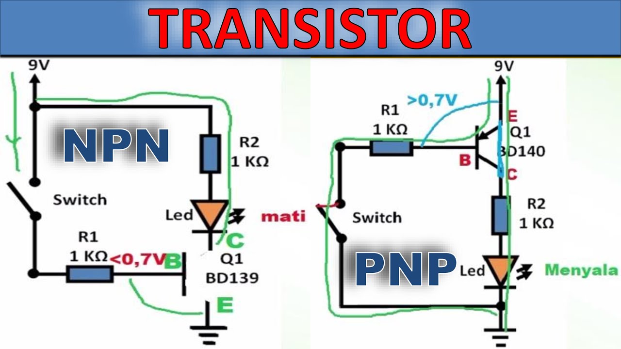
Penjelasan Transistor NPN dan PNP – Beserta contoh rangkaiannya

Como Funciona Un Transistor? ✅️ Bien Explicado‼️

Small Signal Analysis of BJT
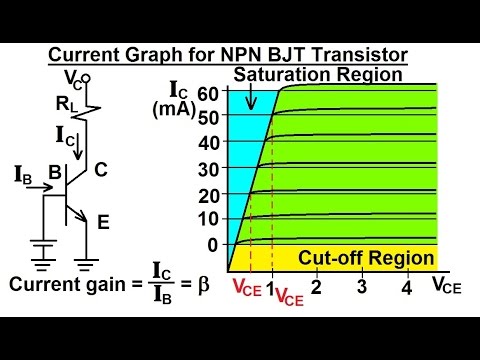
Electrical Engineering: Ch 3: Circuit Analysis (28 of 37) Current Graph for NPN BJT Transistor
5.0 / 5 (0 votes)
