How EUV lithography works
Summary
TLDRThis video script details the intricate process of chip manufacturing, starting with sawing wafers from pure crystalline silicon cylinders. It then describes the use of lithography to print billions of transistors with atomic precision. A high-energy laser creates plasma, which emits extreme ultraviolet light used to etch the circuitry design onto the wafer. The process involves multiple layers and weeks of work, culminating in a fully functional chip with nanometer-scale transistors.
Takeaways
- ⚙️ Wafers are produced by sawing and polishing pure crystalline silicon cylinders to a mirror-like finish.
- 🔍 Lithography is used to print and etch billions of transistors onto a wafer with atomic precision.
- 🌟 A high-energy laser creates plasma from molten tin, emitting extreme ultraviolet light for lithography.
- 🔄 The light beam is reflected and focused into a beam containing the chip's circuitry design.
- 🔬 The pattern of light is shrunk and cast onto the silicon wafer through an array of precise mirrors.
- 🔄 Photoresist is exposed to the light pattern, creating a relief pattern for etching the desired structures.
- 🧼 The wafer is processed and cleaned to remove the resist, preparing it for the next layer.
- 🔁 This process is repeated layer by layer, up to a hundred times, over days or weeks.
- 💾 The end result is a fully functioning chip with transistor dimensions at a nanometer level.
- 🎶 The script is accompanied by music, suggesting a video format.
Q & A
What material is used to create the wafers for semiconductor chips?
-The wafers for semiconductor chips are made from pure crystalline silicon.
How are wafers initially shaped before further processing?
-Wafers are initially sawed out of cylinders of pure crystalline silicon.
What is the purpose of polishing the wafers to a mirror-like finish?
-Polishing the wafers to a mirror-like finish is necessary for the precision required in lithography processes.
What is lithography and how does it relate to chip manufacturing?
-Lithography is a process used to print and etch billions of transistors onto a wafer with atomic precision, which is a crucial step in chip manufacturing.
How is extreme ultraviolet light generated in the chip manufacturing process?
-Extreme ultraviolet light is generated by firing a high-energy laser on a microscopic droplet of molten tin, turning it into plasma.
What is the role of the beam of light in the lithography process?
-The beam of light, which is focused and reflected to contain the complex design of the chip's circuitry, is used to expose the photoresist on the wafer, creating a pattern that can be etched into the silicon.
How is the pattern of light shrunk to the required size for the chip?
-The pattern of light is shrunk through an array of atomically precise reflective mirrors before being cast onto the silicon wafer.
What happens to the photoresist after it is exposed to the light pattern?
-After the photoresist is exposed to the light pattern, it is developed to form a relief pattern that can be used to etch the desired structures into the silicon.
Why is the wafer cleaned after the initial etching process?
-The wafer is cleaned to remove the resist, preparing it for subsequent processing and layering.
How many times is the process repeated to create a fully functioning chip?
-The process is repeated layer after layer, as many as a hundred times, over days and weeks, to create a fully functioning chip.
What is the scale of the transistor dimensions in a fully functioning chip?
-The transistor dimensions in a fully functioning chip are at a nanometer level.
Outlines

Esta sección está disponible solo para usuarios con suscripción. Por favor, mejora tu plan para acceder a esta parte.
Mejorar ahoraMindmap

Esta sección está disponible solo para usuarios con suscripción. Por favor, mejora tu plan para acceder a esta parte.
Mejorar ahoraKeywords

Esta sección está disponible solo para usuarios con suscripción. Por favor, mejora tu plan para acceder a esta parte.
Mejorar ahoraHighlights

Esta sección está disponible solo para usuarios con suscripción. Por favor, mejora tu plan para acceder a esta parte.
Mejorar ahoraTranscripts

Esta sección está disponible solo para usuarios con suscripción. Por favor, mejora tu plan para acceder a esta parte.
Mejorar ahoraVer Más Videos Relacionados
Chip Manufacturing - How are Microchips made? | Infineon
💻 How Are Microchips Made?
Fabricação de Chips - Como Microchips são feitos? - Infineon (Tradução e dublagem: Matteo Reis)

Semiconductor Packaging - ASSEMBLY PROCESS FLOW
How are Microchips Made? 🖥️🛠️ CPU Manufacturing Process Steps
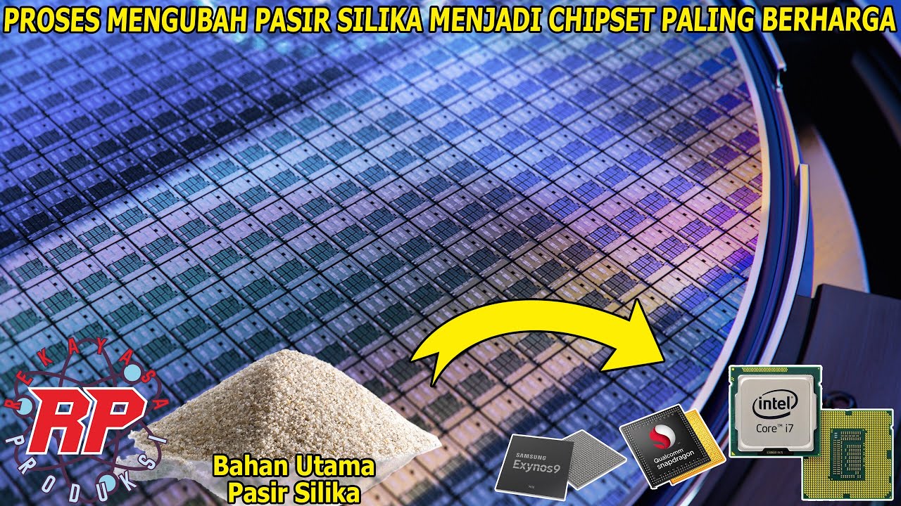
INTIP PROSES PRODUKSI CHIP SEMIKONDUKTOR TERMODERN DARI SILIKON MURNI KE REVOLUSI DIGITAL PROCESSOR
5.0 / 5 (0 votes)
