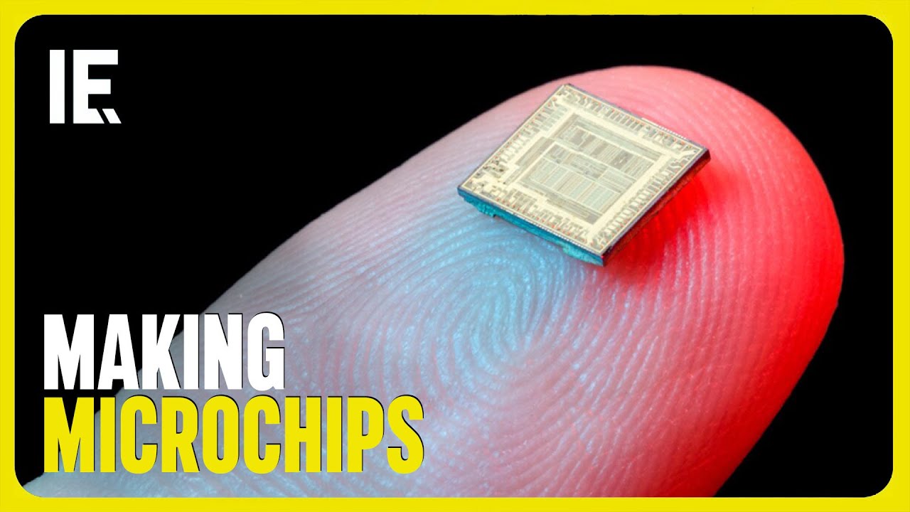
How are Microchips Made? š„ļøš ļø CPU Manufacturing Process Steps
Summary
TLDRThis video script offers an in-depth exploration of microchip manufacturing, detailing the complex process of creating billions of transistors on a tiny chip. It delves into the semiconductor fabrication plant's operations, where silicon wafers undergo around a thousand processes over three months. The script explains the use of high-tech tools, the importance of cleanrooms, and the meticulous steps involved in building layers of metal interconnects and transistors. It also touches on the post-manufacturing testing and categorization of CPUs, providing a comprehensive look at the technology behind our modern devices.
Takeaways
- š± A single smartphone can contain 62 microchips with a total of 90 billion transistors, showcasing the high density of modern technology.
- š Microchips are manufactured in semiconductor fabrication plants, which are vast facilities with clean rooms spanning areas equivalent to 8 football fields.
- š° The machines in these plants are extremely expensive, ranging from a few million to 170 million dollars each, reflecting the high cost of microchip production.
- āļø The production process involves around a thousand steps over a 3-month period, highlighting the complexity and time-consuming nature of microchip manufacturing.
- š¬ Each silicon wafer can be covered in hundreds of CPU chips, each containing 26 billion transistors, indicating the scale of integration in modern chips.
- š The transistors are incredibly small, with FinFETs having dimensions of 36 by 6 by 52 nanometers, emphasizing the nanoscopic precision required.
- š The manufacturing process includes 80 different layers of patterns, each requiring a separate photomask, which are costly and crucial for the design transfer.
- š ļø There are six main groups of semiconductor tools: mask layer creation, material addition, material removal, material modification, wafer cleaning, and wafer inspection.
- š¬ Ion implanters are used to modify the silicon by adding dopants to create P and N regions for transistors, and they are a key part of the front-end manufacturing process.
- š§¼ Cleaning and inspection steps are frequent to ensure the wafer's cleanliness and to check for defects, which is critical for the quality of the final product.
- š The video script took over 1300 hours to create, demonstrating the extensive effort behind producing educational content on complex topics like microchip fabrication.
Q & A
How many microchips are inside the smartphone mentioned in the script?
-There are 62 microchips inside the smartphone.
What is the total number of transistors contained in the microchips of the smartphone?
-The microchips contain a total of 90 billion transistors.
What is the size of a clean room in a semiconductor fabrication plant as described in the script?
-The clean room in a semiconductor fabrication plant spans the area of 8 football fields.
How much does a single machine in the semiconductor fabrication plant cost?
-The cost of a single machine in the semiconductor fabrication plant ranges from a few million to 170 million dollars.
How many processes does a silicon wafer undergo in the microchip manufacturing process?
-A silicon wafer undergoes around a thousand processes in the microchip manufacturing process.
What is the number of CPU chips that can fit on a 300-millimeter silicon wafer?
-A 300-millimeter silicon wafer can fit 230 CPU chips.
How many billions of transistors does each CPU chip contain?
-Each CPU chip contains 26 billion transistors.
How many nanometers are the channel dimensions of the FinFETs transistors mentioned in the script?
-The channel dimensions of the FinFETs transistors are 36 by 6 by 52 nanometers.
What is the total number of metal layers of wires in the CPU described in the script?
-There are a total of 17 metal layers of wires in the CPU.
How many process steps are there in the sequence to build all the 80 layers of the die?
-To build all the 80 layers of the die, there are 940 process steps.
What is the purpose of the cleaning and inspection steps in the microchip manufacturing process?
-The purpose of the cleaning and inspection steps in the microchip manufacturing process is to remove any stray particles that may have fallen onto the wafer and to ensure that each of the processes is being executed with nanometer-level precision.
Outlines
š± Microchip Manufacturing Overview
This paragraph introduces the complexity and scale of microchip manufacturing. It reveals that a single smartphone can contain 62 microchips with a total of 90 billion transistors. The manufacturing process occurs in a semiconductor fabrication plant, which is a vast, clean environment filled with expensive machinery. The process involves around a thousand steps over a 3-month period, resulting in silicon wafers covered in hundreds of CPU chips, each with billions of transistors. The video promises to explore this intricate process, including the nanoscopic transistors and the complex 3D wiring.
š Inside the Microchip Factory
The second paragraph delves into the analogy of microchip manufacturing to baking an 80-layer cake with precise requirements. It outlines the steps to create a single layer of an integrated circuit, starting with the deposition of insulating silicon dioxide and photoresist, followed by patterning with UV light and etching. The paragraph emphasizes the complexity and precision required, with 940 steps repeated to build all layers. It also introduces the semiconductor fabrication plant's operations, including the transportation of silicon wafers and the use of various tools, each performing a specific process step.
š ļø Semiconductor Tools and Their Functions
This paragraph discusses the different types of semiconductor tools used in the fabrication process, categorized by their functions. It explains the role of each tool group, such as creating mask layers, adding or removing materials, modifying the silicon, cleaning the wafers, and inspecting for defects. The paragraph provides a detailed look at the photolithography tool, which is crucial for transferring designs onto the wafer. It also touches on the variety of deposition tools and their role in adding materials to the wafer based on the mask layer.
š¬ Detailed Process of Wafer Processing
The fourth paragraph focuses on the detailed process of how semiconductor tools process the wafer to create a single metal interconnect layer. It describes the steps of insulating layer deposition, photoresist application, photolithography, etching, and chemical mechanical planarization (CMP). The paragraph also highlights the importance of cleaning and inspection steps to ensure the quality of the integrated circuit. Additionally, it mentions the complexity of fabricating FinFET transistors and the need for additional steps not covered in the summary.
š Behind the Scenes of Microchip Manufacturing
This paragraph provides insight into the efforts behind creating the video, including the extensive research, modeling, scripting, and animation that took over 1300 hours. It emphasizes the secrecy surrounding the semiconductor industry's processes and tools. The paragraph also discusses the additional steps in microchip manufacturing, such as silicon wafer production and post-fabrication testing. It concludes with a call to action for viewers to support the creators through likes, subscriptions, and Patreon, and mentions the sponsor, Brilliant.org, which offers educational resources on various technology topics.
š Learning Resources and Future Content
The final paragraph promotes Brilliant.org as a learning resource for complex technology concepts, including AI and large language models. It mentions a specific course on technology that covers topics like GPS, computer memory, and recommendation algorithms. The paragraph also discusses the creators' plans for future videos on microchip fabrication, transistor physics, GPUs, and CPU architecture. It expresses gratitude to supporters and sponsors and encourages viewers to subscribe for updates on new content.
Mindmap
Keywords
š”Microchips
š”Transistors
š”Semiconductor Fabrication Plant
š”Clean Room
š”Silicon Wafers
š”Integrated Circuit
š”Photolithography
š”FinFET
š”Ion Implantation
š”Chemical Mechanical Planarization (CMP)
š”Metrology Tools
Highlights
A smartphone contains 62 microchips with a total of 90 billion transistors.
Microchips are manufactured in semiconductor fabrication plants with clean rooms spanning the area of 8 football fields.
Silicon wafers undergo around a thousand processes over a 3-month period in the fabrication process.
Each silicon wafer ends up covered in hundreds of CPU chips, each containing 26 billion transistors.
The nanoscopic transistors and layers of wires form an integrated circuit that is cut, tested, and packaged for use in computers.
A CPU chip has 24 cores, a memory controller, a graphics processor, and other sections, with 44,000 transistors in a single multiply block.
Transistors are incredibly small, with FinFETs having channel dimensions of 36 by 6 by 52 nanometers.
The manufacturing process is compared to baking an 80-layer cake with unique shapes and 940 steps, taking 3 months to complete.
A single layer of the integrated circuit involves depositing insulating silicon dioxide, applying photoresist, and using UV light for patterning.
The semiconductor fabrication plant uses a variety of machines, each costing between a few million to 170 million dollars.
Silicon wafers are transported in a cleanroom using a front opening universal pod (foup) and an overhead transport system.
The fabrication plant has 435 semiconductor tools that can produce 50,000 wafers or 11.5 million CPUs a month.
Semiconductor tools are categorized into six groups: making the mask layer, adding material, removing material, modifying the material, cleaning the wafer, and inspecting the wafer.
Photolithography tools use UV light and photomasks to transfer designs onto wafers for nanoscopic patterning.
Deposition tools add materials like metals, insulators, and crystalline layers of silicon onto the wafer using a mask layer.
Etching and chemical mechanical planarization (CMP) are used to remove material and ensure a flat wafer surface for additional layers.
Ion implanters modify the silicon by bombarding it with elements like phosphor or boron to form the transistors.
Wafer washers clean the wafer to remove contaminants, and metrology tools inspect for defects with nanometer-level resolution.
The manufacturing process of a single metal interconnect layer involves multiple steps, including deposition, etching, and planarization.
The video's creation took over 1300 hours of research, modeling, scripting, and animation to provide detailed insights into microchip manufacturing.
The video is sponsored by Brilliant.org, which offers interactive learning modules on various scientific and technological topics.
Transcripts
Inside this smartphone are 62 microchipsĀ containing a total of 90 billion transistors.Ā Ā
These microchips are incredibly powerful andĀ the cornerstone of all technology, but how areĀ Ā
billions of nanoscopic transistors manufacturedĀ into a microchip the size of a tiny ant?Ā
Well, all these microchips were manufactured inĀ a semiconductor fabrication plant like this one.Ā Ā
Inside it is a clean room which spans the area ofĀ 8 football fields and is filled with hundreds ofĀ Ā
machines ranging in size from that of a van toĀ that of a city bus and costing anywhere betweenĀ Ā
a few million and 170 million dollars. WithinĀ this microchip factory, silicon wafers travelĀ Ā
from machine to machine and undergo around aĀ thousand processes over a 3-month period. And,Ā Ā
by the end of production, each silicon waferĀ will be covered in hundreds of CPU chipsĀ Ā
each containing 26 billion transistors. When we zoom in we can see the nanoscopicĀ Ā
transistors at the bottom and overĀ a dozen layers of wires above. ThisĀ Ā
integrated circuit is then cut out fromĀ the wafer, tested, and packaged so thatĀ Ā
it can be installed into your desktop computer. In this video weāre going to explore the entireĀ Ā
microchip manufacturing process and showĀ you how billions of nanoscopic transistorsĀ Ā
and an impossibly complex 3D maze of wiresĀ are manufactured in one of the worldās mostĀ Ā
technologically advanced microchip factories.Ā Itās an incredibly complicated process,Ā Ā
so stick around and letās jump right in! A portionĀ of this video is sponsored by Brilliant.org.Ā
There are two sides to understanding how microchipĀ manufacturing works. The first is the sequence ofĀ Ā
steps and processes needed to build the nanoscopicĀ transistors and the labyrinth of wires. WhereasĀ Ā
the second is how the semiconductor fab andĀ multimillion dollar equipment on the cleanroomĀ Ā
floor work, and weāll be flipping betweenĀ these two sides to get a complete picture.Ā
Letās start by opening up this desktop computer,Ā focusing on the CPU and taking a look at whatāsĀ Ā
inside. Here we have an integrated circuit, orĀ die, which weāll refer to as a chip. This chipĀ Ā
has 24 cores, a memory controller, a graphicsĀ processor, and many other sections. Within oneĀ Ā
of the cores, we can see its block diagramĀ and the various elements. Zooming in onĀ Ā
this multiply block, we find a layout of 44Ā thousand transistors that physically executeĀ Ā
32-bit multiplication and constitute justĀ point zero zero zero one seven percent of theĀ Ā
overall 26 billion transistors in the CPU. Zooming in even further, we see layers ofĀ Ā
metal wires, or interconnects, and at the veryĀ bottom are the transistors that form the basicĀ Ā
logic gates. Note that these layers of metalĀ interconnects arenāt floating, but rather,Ā Ā
the empty space that you see is filled withĀ insulating materials, thus providing structure,Ā Ā
and preventing the metal wire layers fromĀ touching. Furthermore, here weāre only showingĀ Ā
the transistors at the bottom and five layers ofĀ metal interconnects with vias traveling verticallyĀ Ā
between the layers. In actuality there are aĀ total of 17 metal layers of wires in the CPU,Ā Ā
and each successive set of levels uses largerĀ and larger interconnects. At the bottom areĀ Ā
local interconnects that move data around thisĀ 32 bit multiply circuit. In the middle areĀ Ā
intermediate interconnects that move data aroundĀ the core, and at the top are global interconnectsĀ Ā
that move data around the entire CPU. You might be wondering how small areĀ Ā
these transistors? Zooming in again and pastĀ the interconnect layers we find FinFets,Ā Ā
which are transistors whose channel dimensionsĀ are 36 by 6 by 52 nanometers with a transistorĀ Ā
to transistor pitch of 57 nanometers. ClearlyĀ the transistors are incredibly small. HereāsĀ Ā
a mitochondria, a dust particle, andĀ a human hair for size comparisons.Ā
Now that you have a sense of what the transistorsĀ and labyrinth of metal interconnects look like,Ā Ā
letās explore how theyāre manufactured. Weāll begin with an analogy. Imagine bakingĀ Ā
a cake thatās 80 layers tall, with each layer cutĀ to a unique shape. To make this cake there areĀ Ā
940 steps in the recipe, which takes 3 monthsĀ to complete and includes hundreds of exoticĀ Ā
ingredients. And, if any measurement, bakingĀ time, or temperature is more than one percent off,Ā Ā
then the cake is entirely ruined. ThatāsĀ kind of what itās like to make a microchip,Ā Ā
but microchips are even more complicated. Letās look at a single layer of this integratedĀ Ā
circuit and run through a simplifiedĀ set of steps used to build it. To start,Ā Ā
a layer of insulating silicon dioxide is depositedĀ on top of the wafer and then a layer of lightĀ Ā
sensitive photoresist is spread across the top.Ā Next, using UV Light and a stencil, a pattern isĀ Ā
applied to the photoresist. Solvents then areĀ used to remove the areas hit by the UV light,Ā Ā
thus creating a patterned mask layer. Using theĀ mask, the revealed silicon dioxide is etched awayĀ Ā
down to the previous layer. Next the mask layer isĀ removed, and a layer of copper is added to coverĀ Ā
the wafer and fill in the areas that were justĀ etched away. Finally, the surface is ground downĀ Ā
and leveled off to reveal the copper and insulatorĀ patterns. And thus, a single layer is completed.Ā
In order to build the next layer, which isĀ a vertical set of metal vias, we repeat theĀ Ā
same set of steps, but use a different patternĀ for the photomask. Since these layers are allĀ Ā
built using the same set of steps itās moreĀ effective to visualize the steps as a circleĀ Ā
like a clock. To build all the 80 layers of theĀ die, this sequence is repeated over and over,Ā Ā
resulting in 940 steps. One important note isĀ that the FinFet transistors at the bottom areĀ Ā
even more complicated than the metal wires, andĀ thus additional steps are needed to fabricateĀ Ā
them. Furthermore, cleaning the wafer to wash awayĀ dust particles that may have landed on the wafer,Ā Ā
as well as inspecting the wafer to makeĀ sure everything is being built properly,Ā Ā
happens frequently and these steps need toĀ be added to the circle. A different tool isĀ Ā
used to complete each of these process steps. . Now that we have an understanding of the steps,Ā Ā
letās take a look at this semiconductorĀ fabrication plant. This CPU is manufacturedĀ Ā
on a 300-millimeter silicon wafer which canĀ fit 230 CPU chips. In contrast DRAM chips areĀ Ā
considerably smaller and thus 952 of them can fitĀ on a wafer. These silicon wafers are carried inĀ Ā
stacks of 25 using a container called a frontĀ opening universal pod, or foup. This sealedĀ Ā
plastic wafer carrier is transported around theĀ cleanroom floor using an overhead transport systemĀ Ā
which lowers the foup onto the toolās landing pad.Ā Inside the tool, robotic arms transport the waferĀ Ā
through vacuum load locks and to differentĀ process chambers where materials are added,Ā Ā
removed, or processed in ways that weāll exploreĀ later. The wafers are then returned to the foup,Ā Ā
resealed inside, lifted up to the overheadĀ transport system, and carried to and droppedĀ Ā
onto the next tool, where the next step in theĀ process is completed. To build the entire chipĀ Ā
composed of 80 different layers it takes 3 monthsĀ of traveling from tool to tool where at eachĀ Ā
stop one of the 940 process steps is completed. In order to increase the microchip mass productionĀ Ā
capabilities of a semiconductor fabricationĀ plant or fab, typically there are dozens of theĀ Ā
same semiconductor tools organized in rows thatĀ perform the same process. On the cleanroom floorĀ Ā
there are a total of 435 semiconductor toolsĀ resulting in the fabās production capacity ofĀ Ā
50,000 wafers or 11.5 million CPUs a month. These tools have rather complicated names,Ā Ā
so weāll start by categorizing them accordingĀ to their functionality. There are 6 groups:Ā Ā
making the mask layer, adding material,Ā removing material, modifying the material,Ā Ā
cleaning the wafer, and finally inspectingĀ the wafer. Weāve color coded the differentĀ Ā
functional groups to the various tools andĀ process steps to help you not get lost.Ā
Letās next look at each of these semiconductorĀ tools and see how they process the wafer inĀ Ā
various ways. Weāll start with the ones that areĀ used to make the mask layer or the nanoscopicĀ Ā
stencil on the wafer. These tools include theĀ photoresist spin coater, photolithography tool,Ā Ā
developer and photoresist stripper. First theĀ photoresist spin coater applies a light-sensitiveĀ Ā
layer to the surface of the wafer and sendsĀ it through a soft bake where the wafer isĀ Ā
heated in order to evaporate the solvent fromĀ the photoresist. Next the wafer goes to theĀ Ā
lithography tool which shines UV light through aĀ stencil, which is technically called a photomask.Ā Ā
The light passes through the stencil and is thenĀ demagnified or shrunk down to produce a nanoscopicĀ Ā
pattern on the wafer. Wherever the light fromĀ the stencil touches the wafer, the photoresist isĀ Ā
weakened. The wafer then goes to the developerĀ and the weakened photoresist is washed away,Ā Ā
leaving only the patterned nanoscopic stencil onĀ the wafer. The wafer is then sent through a hardĀ Ā
bake to harden the remaining photoresist.Ā Next the wafer travels to other tools toĀ Ā
undergo processing, and once these processesĀ are completed the wafer goes to a photoresistĀ Ā
stripper which uses solvents to dissolve andĀ remove the photoresist mask layer. And thatāsĀ Ā
how a mask layer is formed and then removed. The photolithography tool is one of the mostĀ Ā
important, so letās take a look at it. InsideĀ is a UV light source, a set of lenses toĀ Ā
focus the light, a photomask which contains theĀ stencil, or design of the layer to be patterned,Ā Ā
and a wafer carrier. The photomask is 6 by 6Ā inches, and, based on the dimensions of the CPU,Ā Ā
can fit 2 copies of a single layer ofĀ the CPU design. The purpose of usingĀ Ā
a photomask with these crazy optics is becauseĀ itās a reliable way to copy and paste a designĀ Ā
for billions of nanoscopic transistors and wiresĀ onto 230 identical CPUs on a single wafer in aĀ Ā
few minutes. After the light passes through theĀ photomask, the UV light goes to more lenses inĀ Ā
order to shrink down the pattern by a factor ofĀ 4 and print a single layer of the design onto theĀ Ā
photoresist. The wafer carrier steps from positionĀ to position, printing the photomask image at eachĀ Ā
stop, until all 230 chips are patterned. Letās clarify one detail. In our previousĀ Ā
examples, we talked a lot about this CPU having 80Ā layers. Specifically, what we were referring to isĀ Ā
the number of photomasks and mask layers used toĀ create all the different layers of patterns onĀ Ā
the wafer. Therefore, one complete CPU chipĀ uses 80 different photomasks, each costingĀ Ā
300,000 dollars. With only one mask layer beingĀ patterned at a time, this CPU chip will undergo 80Ā Ā
separate visits to the lithography tool. We couldĀ spend another hour talking about photolithographyĀ Ā
but letās move onto the next category of tools. Deposition tools are used to add or depositĀ Ā
material onto the wafer. A lot of times weĀ use the mask layer from the photolithographyĀ Ā
step to add materials to the areas uncoveredĀ by the mask layer, kind of like spray paintingĀ Ā
through a stencil. Due to the wide range ofĀ elements and compounds used to create the layers,Ā Ā
deposition tools have a wide range of variationsĀ with complicated names and acronyms for eachĀ Ā
variant. But essentially there are 3 key groupsĀ of materials that are added or deposited ontoĀ Ā
the wafer: metals such as copper or tantalum,Ā insulators which are typically called oxides,Ā Ā
and crystalline layers of silicon. Each group ofĀ different materials uses different physics andĀ Ā
chemistry principles to deposit the materialĀ on the wafer and therefore has a differentĀ Ā
technical name for the tool that deposits theĀ material. Deposition tools typically have aĀ Ā
central wafer handling chamber, with the variousĀ chambers attached to the edges, each one dedicatedĀ Ā
to adding just a single element or compound. The next category of machines do the opposite,Ā Ā
which is to remove material. There are 2Ā key methods. The first is etching. EtchersĀ Ā
use either corrosive chemicals or high energyĀ plasmas to react with and remove materials fromĀ Ā
the surface of the wafer. They are typically usedĀ with the mask layer stencil in order to remove theĀ Ā
material exposed by the mask, thus creating a holeĀ that can be later filled by a deposition tool.Ā
The second method to remove material is CMP,Ā which is chemical mechanical planarization. CMPĀ Ā
applies slurry and uses abrasive pads to grindĀ and polish away the top surface of the wafer,Ā Ā
making it perfectly flat. CMP levels off the topĀ layers of the wafer and is typically used as theĀ Ā
last step in a cycle of processes in order toĀ prepare the wafer for another layer to be added.Ā
The fourth category are tools that modify theĀ silicon and are called ion implanters. These toolsĀ Ā
use the photomask stencil to bombard the unmaskedĀ regions with phosphor, boron, or other elementsĀ Ā
in order to make the P and the N regions requiredĀ to form the transistors themselves. Therefore, ionĀ Ā
implanters are only used in the front end of line.Ā You might think that this is adding material.Ā Ā
However, ion implanters only add around one atomĀ of phosphor or boron for every 10,000 atoms ofĀ Ā
silicon. Additionally, while other machines sprayĀ paint a layer on top of the wafer, ion implantersĀ Ā
hurl atoms deep into the silicon lattice, kindĀ of like a cannon launching a baseball 6 feet intoĀ Ā
a concrete wall. This process typically damagesĀ the silicon lattice, which is why the followingĀ Ā
step is to repair the silicon by heating theĀ wafer using a separate tool called an annealer.Ā
The fifth category of tools are used to cleanĀ and remove any contaminants or particles from theĀ Ā
wafer. These wafer washers use ultra-pure water toĀ clean the wafer and then dry it with nitrogen orĀ Ā
hot isopropyl alcohol. Cleaning the wafer happensĀ rather frequently in order to remove any strayĀ Ā
particles that may have fallen onto the wafer. And finally, sixth are tools that inspect theĀ Ā
transistors and metal layers for defects andĀ are called metrology tools. A common metrologyĀ Ā
tool uses a scanning electron microscope withĀ nanometer-level resolution to take pictures of theĀ Ā
top surface of the wafer and determine if thereĀ are defects such as improperly patterned layersĀ Ā
or particles on the surface. When fabricatingĀ an integrated circuit that takes 3 months toĀ Ā
complete, itās important to repeatedly monitor theĀ progress and make sure that each of the processesĀ Ā
is being executed with nanometer-level precision. Now that weāve covered each of the categories,Ā Ā
here are the color coded process stepsĀ along with the layout of the tools in theĀ Ā
semiconductor fabrication plant. Letās runĀ through the complete set of steps used toĀ Ā
manufacture a single metal interconnect layer. First a layer of insulating silicon dioxide isĀ Ā
deposited onto the wafer. Next photoresist isĀ spread across the surface and the wafer is sentĀ Ā
through a soft bake to remove the solvent. TheĀ wafer then travels to the photolithography toolĀ Ā
where the design from the photomask is transferredĀ to each of the chips on the wafer by weakeningĀ Ā
the areas of photoresist hit by the light. TheĀ wafer next goes to the developer to wash awayĀ Ā
the sections that were hit by the light from theĀ lithography tool and then through a hard bake toĀ Ā
harden the remaining photoresist. With the maskĀ layer built, the wafer goes to an etching tool,Ā Ā
where a plasma etcher removes a vertical columnĀ through the exposed silicon dioxide until itĀ Ā
reaches the previous layerās metal vias. Next theĀ wafer is sent to a photoresist stripper where theĀ Ā
mask layer is removed. The wafer then travelsĀ to a physical vapor deposition tool where aĀ Ā
sequence of metals fills in the exposed patternĀ and coats the wafer in metal. Finally the waferĀ Ā
is sent to a chemical mechanical planarizationĀ tool where the metal is ground down so that allĀ Ā
that remains is a flat layer of insulating siliconĀ dioxide and conductive copper interconnects thatĀ Ā
match the pattern from the photomask. A singleĀ metal layer is now completed, and the wafer isĀ Ā
ready for the next cycle to begin where insulatingĀ silicon dioxide and the vias will be added. NoteĀ Ā
that cleaning and wafer metrology or inspectionĀ steps occur in between many of these otherĀ Ā
steps. Furthermore, the process steps to make theĀ transistors are less straightforward and utilizeĀ Ā
the ion implanter, and thus weāll cover them in aĀ separate video on transistor physics and design.Ā
These steps are for building theĀ integrated circuit on the wafer, however,Ā Ā
there are additional steps in manufacturing aĀ microchip which weāll explore in a little bit.Ā
But before we get there, one important thingĀ to note is that the semiconductor industryĀ Ā
is incredibly secretive regarding the exact toolĀ layout and the process steps and recipes used toĀ Ā
make the transistors. We wanted to make the bestĀ video on how microchips are made and it took usĀ Ā
180 hours of scouring the internet and textbooksĀ for information and reference images and, usingĀ Ā
what we found, we spent 205 hours modeling eachĀ of these tools, the many layers of the integratedĀ Ā
circuit, and the semiconductor fab. Furthermore,Ā writing the script took about 100 hours, and thenĀ Ā
animating all these visuals took more than 825Ā hours. As a result, this video took over 1300Ā Ā
hours to make, and itās entirely free to watch.Ā We want to make more videos like this one where weĀ Ā
explore computer architecture and how transistorsĀ work, and we canāt do it without your help. TheĀ Ā
best way you can help is by taking a few secondsĀ to scroll down, write a comment below, like thisĀ Ā
video, subscribe if you havenāt already and thenĀ share this video on social media or send it to aĀ Ā
friend or colleague. Truly, just a few secondsĀ of your time helps far more than you think.Ā Ā
Additionally, we have a Patreon page whereĀ weāll be releasing behind the scenes footageĀ Ā
of our work and updates for upcomingĀ videos. If you find what we do useful,Ā Ā
we would appreciate any support. Thank you. So then, what are the additional steps inĀ Ā
manufacturing a microchip? BeforeĀ chip manufacturing at the fab,Ā Ā
we first have to manufacture the siliconĀ wafers by refining quartzite into pure silicon,Ā Ā
and then growing a monocrystalline ingotĀ and cutting it into wafers. For reference,Ā Ā
these 300-millimeter wafers are aroundĀ three-quarters of a millimeter thick,Ā Ā
they have a barcode on the side and a smallĀ notch in them to indicate the direction of theĀ Ā
crystal lattice. Furthermore, these wafers areĀ incredibly delicate, and shatter into hundredsĀ Ā
of shards when broken. A single wafer costsĀ around a hundred dollars, but after beingĀ Ā
populated with CPUs itās worth closer to a hundredĀ thousand dollars, making it quite literally tenĀ Ā
times more valuable than its weight in gold. Moving onto the steps after chip manufacturing.Ā Ā
The completed wafer is sent to a separate buildingĀ where each of the CPUs undergoes rigorous testingĀ Ā
to figure out if it works as intended. If a CPUĀ works, thatās great. But frequently a particleĀ Ā
or photomask defect has damaged a section ofĀ the integrated circuit, rendering that sectionĀ Ā
defective. These semi-functional circuits are thenĀ categorized, or binned, based on what still works.Ā Ā
These Intel Thirteenth Gen processors are sold asĀ an i9, i7, i5, or i3, depending on how many coresĀ Ā
are functional with different product lines ofĀ CPUs whose on-board integrated graphics sectionsĀ Ā
are defective. These wafers are transportedĀ to another building where the chips are cutĀ Ā
out using a laser, flipped over, and placed on anĀ interposer which distributes the connection pointsĀ Ā
to a printed circuit board while a protectiveĀ heat conductive cover is placed on the backĀ Ā
side. The printed circuit board holds the landingĀ grid array that interfaces with the motherboardĀ Ā
as well as various electrical components. NextĀ an integrated heat spreader is mounted on top,Ā Ā
and the entire assembly is tested one last timeĀ before being packaged for sale. Finally, the CPUĀ Ā
is now ready to be mounted onto the motherboardĀ and installed into your desktop computer.Ā
Itās important to understand that chipĀ manufacturing requires an incredibleĀ Ā
amount of science and engineering and thereās aĀ free and easy way to learn the basic principlesĀ Ā
inside each of these complex tools and thatās withĀ this videoās sponsor, Brilliant.org! BrilliantĀ Ā
reimagines how courses are taught. InsteadĀ of boring hour-long lectures or textbooksĀ Ā
that put you to sleep, Brilliant uses fun andĀ interactive modules inside thousands of lessonsĀ Ā
from basics to advanced topics ā and new lessonsĀ are added every month. Whatever your skill level,Ā Ā
Brilliant customizes its content to fit yourĀ needs and allows you to learn at your own pace.Ā
We use Brilliant daily. Weāre working onĀ videos on how AI and Chat GPT Works, andĀ Ā
so each of our animators is progressing throughĀ their lessons on How Large Language Models work.Ā
Because youāre watching this video, you probablyĀ enjoy learning about how technology works,Ā Ā
and fortunately for you, Brilliant just addedĀ a course on this very topic. In it they haveĀ Ā
lessons such as How GPS Works, How ComputerĀ Memory Works, and how Recommendation AlgorithmsĀ Ā
such as those used by YouTube work. IfĀ youāre looking to advance your career,Ā Ā
Brilliant is the go-to resource for leveling upĀ your skills and staying up-to-date on the latestĀ Ā
concepts behind world-changing technology. For the viewers of this channel, BrilliantĀ Ā
is offering a free 30-day trial with access toĀ all their thousands of lessons. Additionally,Ā Ā
Brilliant is offering 20% off anĀ annual subscription. Just go toĀ Ā
brilliant.org/brancheducation. TheĀ link is in the description below.Ā
Microchip Fabrication is a massive topic, andĀ thus, we have two more equally complex videosĀ Ā
that weāre working on. The first will be anĀ in-depth 3D animated factory tour and theĀ Ā
second will explore transistor physics, FinFets,Ā and the next generation of transistors. WeāreĀ Ā
also working on a series of videos on GPUs and aĀ separate one on CPU architecture so make sure toĀ Ā
subscribe so you donāt miss any of our videos. Weāre thankful to all our Patreon and YouTubeĀ Ā
Membership Sponsors for supporting our work.Ā If you want to financially support our work,Ā Ā
you can find the links in the description below. This is Branch Education, and we create 3DĀ Ā
animations that dive deeply into the technologyĀ that drives our modern world. Watch another BranchĀ Ā
video by clicking one of these cards or clickĀ here to subscribe. Thanks for watching to the end!
Browse More Related Video
š» How Are Microchips Made?
How EUV lithography works
SMIC making a 3nm Chip for Huawei | China Semiconductor | Space Tech & Military Innovation AI
Computers, Circuit Boards, Flash Drives & More | How It's Made | Science Channel
How it's Made ? Cotton cloth || ą¤ą¤Ŗą¤¾ą¤ø ą¤øą„ ą¤ą¤Ŗą¤”ą¤¼ą¤¾ ą¤¬ą¤Øą¤¾ą¤Øą„ ą¤ą„ ą¤Ŗą„ą¤°ą¤ą„ą¤°ą¤æą¤Æą¤¾ || Farming Engineer ||
How a CPU is made
5.0 / 5 (0 votes)