Kicad Beginner Tutorial- A Traffic Light for Arduino ( RE-UPLOADED, Twice )
Summary
TLDRThis video demonstrates the process of creating and designing a PCB (Printed Circuit Board) using KiCad, focusing on laying out the components efficiently for easy assembly and understanding. The tutorial covers tips on adjusting component placement for clarity, such as aligning resistors with their values, enhancing visual organization, and improving labeling. The presenter shares helpful tricks for optimizing the design, including simplifying the view for easier navigation. Viewers are encouraged to subscribe for more tutorials, including upcoming coding and FreeCAD videos, making this a practical resource for both beginners and experienced users.
Takeaways
- 😀 KiCad is an open-source tool for designing PCBs and creating circuit layouts.
- 😀 The tutorial focuses on creating a simple circuit with LEDs, resistors, and a 4-pin connector.
- 😀 The video covers how to create a schematic, place components, and wire them together in KiCad.
- 😀 The tutorial highlights the importance of assigning footprints to components for accurate PCB design.
- 😀 The 3D viewer in KiCad helps visualize the PCB design and ensures proper component alignment.
- 😀 KiCad’s PCB editor allows easy placement and routing of traces for the circuit board.
- 😀 Using the 3D viewer, you can verify the design from different angles before finalizing the layout.
- 😀 The video emphasizes the importance of neat component placement for a clean PCB layout.
- 😀 Adding labels and adjusting the board edges helps make the PCB more professional and readable.
- 😀 The host mentions plans to cover more KiCad tutorials, along with FreeCAD and coding videos in future content.
- 😀 Viewers are encouraged to subscribe and click the notification bell to stay updated on upcoming tutorials.
Q & A
What is the primary focus of this KiCad tutorial?
-The tutorial focuses on creating a simple schematic and circuit board using KiCad, with an emphasis on beginner-level concepts. It covers basic components such as LEDs, resistors, a connector, and mounting holes.
What are symbols in KiCad, and how are they used in the schematic?
-In KiCad, symbols represent components in a schematic. They are used to visually depict electrical components like resistors, LEDs, and connectors. These symbols are placed on the schematic before generating the physical PCB layout.
What does the term 'footprint' mean in KiCad, and why is it important?
-A 'footprint' in KiCad refers to the physical layout of a component on the PCB, including pad sizes, spacing, and mounting hole positions. It is important because it defines how the components will be physically placed and connected on the board.
How do you add components to the schematic in KiCad?
-To add components to the schematic in KiCad, you use the symbol tool, which allows you to search for and select components like LEDs, resistors, and connectors from the symbol library. Once selected, they can be placed on the schematic.
What is the process of annotating a schematic in KiCad?
-Annotating a schematic in KiCad involves assigning unique reference designators (like R1, D1, etc.) to each component. This is done by using the 'Annotate' tool, which automatically changes the question marks next to components into numbered references.
What is the function of the 'CVPCB' tool in KiCad?
-The 'CVPCB' tool in KiCad is used to assign footprints to the components in the schematic. This process connects the electrical symbols to their physical counterparts, which are later used in the PCB layout.
How do you perform a basic electrical check in KiCad?
-In this tutorial, a basic electrical rules check (ERC) is not performed since the circuit is simple. However, for more complex circuits, KiCad provides the ERC tool to identify electrical issues like unconnected pins or conflicting connections.
What is the role of the 3D viewer in KiCad?
-The 3D viewer in KiCad allows users to visualize their PCB layout in three dimensions. It provides a realistic view of the circuit board, helping users check component placements, trace routing, and overall design aesthetics.
Why is it important to assign the correct footprint to components?
-Assigning the correct footprint to components is essential for ensuring that the physical components will fit correctly on the PCB during manufacturing. Incorrect footprints can result in components not fitting or not aligning with pads, leading to assembly issues.
What is the process for running traces in KiCad's PCB layout tool?
-To run traces in KiCad, you select the 'Route Tracks' tool, which allows you to connect the pads of components with copper traces. The tool automatically guides the trace routing, but users can manually adjust the paths for optimal layout.
Outlines

هذا القسم متوفر فقط للمشتركين. يرجى الترقية للوصول إلى هذه الميزة.
قم بالترقية الآنMindmap

هذا القسم متوفر فقط للمشتركين. يرجى الترقية للوصول إلى هذه الميزة.
قم بالترقية الآنKeywords

هذا القسم متوفر فقط للمشتركين. يرجى الترقية للوصول إلى هذه الميزة.
قم بالترقية الآنHighlights

هذا القسم متوفر فقط للمشتركين. يرجى الترقية للوصول إلى هذه الميزة.
قم بالترقية الآنTranscripts

هذا القسم متوفر فقط للمشتركين. يرجى الترقية للوصول إلى هذه الميزة.
قم بالترقية الآنتصفح المزيد من مقاطع الفيديو ذات الصلة

How to Make an Automatic Emergency Light || Power Failure Backup Light

Merancang dan Membuat Single/ Double Layer PCB secara Manual dengan Metode Eksposure

12 Menit Tutorial Desain PCB Eagle 7.6.0

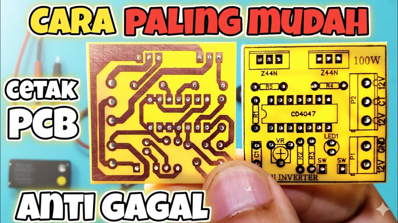
CARA CETAK PCB MANUAL Paling mudah anti gagal

Surface Mount Assembly Process Step by Step

Electronic project // Simple Door Security alarm System // New Electrical project // Buzzer project.
5.0 / 5 (0 votes)
