Common Emitter Configuration with input and output characteristics in Telugu//EC&PS//diploma//B.tech
Summary
TLDRIn this video, the concept of the **Common Emitter Configuration** in transistors is explained for first-year diploma students in Electronics and Communication. The configuration, where the emitter terminal is common to both the input and output, is crucial for understanding transistor operation in amplification circuits. The video covers the relationships between base-emitter voltage (V_BE), base current (I_B), collector-emitter voltage (V_CE), and collector current (I_C), along with key formulas for calculating input and output resistance. It also explores the transistor's behavior in different regions: cutoff, active, and saturation. The content concludes by inviting viewers to continue learning with the next video on the Common Collector Configuration.
Takeaways
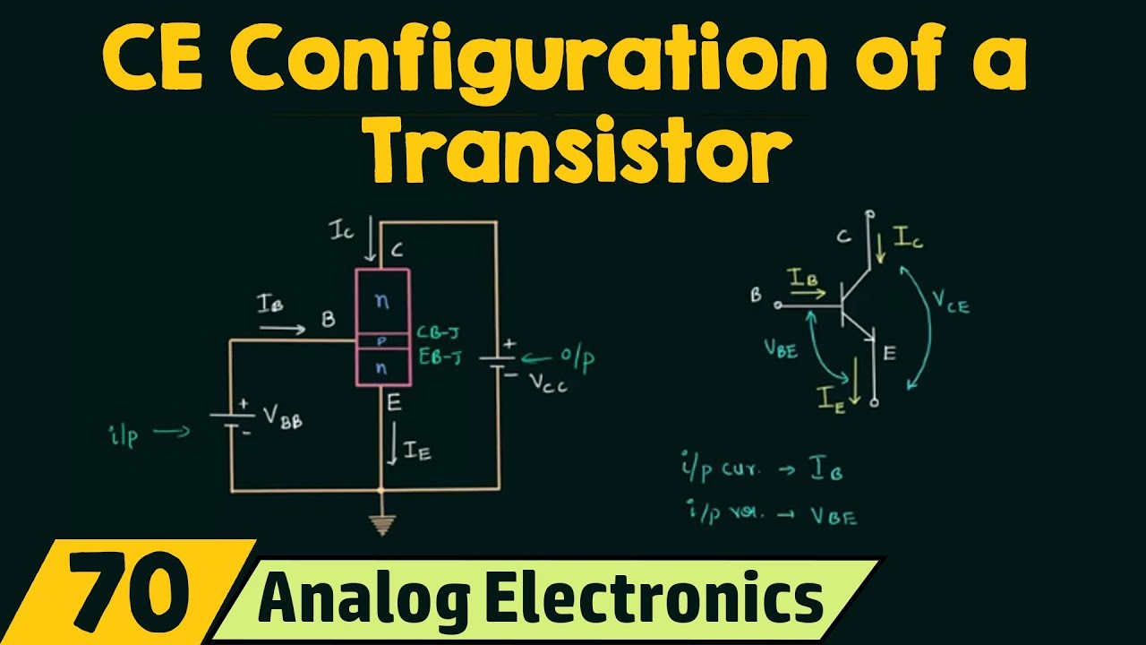
- 😀 Common Emitter Configuration: The common emitter configuration is used in electronics where the emitter terminal is connected to ground, making it a grounded emitter configuration.
- 😀 NPN Transistor: In the common emitter configuration, the transistor used is typically an NPN transistor, which has three terminals: emitter, base, and collector.
- 😀 Input and Output Characteristics: In the common emitter configuration, the input characteristics are drawn between the base current (Ib) and base-emitter voltage (Vbe), while the output characteristics are drawn between collector current (Ic) and collector-emitter voltage (Vce).
- 😀 Constant Parameters: When plotting input characteristics, the collector-emitter voltage (Vce) is kept constant. For output characteristics, the base current (Ib) is kept constant.
- 😀 Input Resistance Formula: The input resistance (Ri) can be calculated using the formula Ri = ΔVbe / ΔIb, which is the ratio of the change in base-emitter voltage to the change in base current at a constant Vce.
- 😀 Output Resistance Formula: The output resistance (Ro) is calculated as Ro = ΔVce / ΔIc, which is the ratio of the change in collector-emitter voltage to the change in collector current at a constant Ib.
- 😀 Regions of Operation: The common emitter transistor has three regions: cut-off, active, and saturation. The transistor operates in active mode when the base-emitter junction is forward biased and the collector-emitter junction is reverse biased.
- 😀 Cut-off Region: The transistor operates in the cut-off region when both the base-emitter and collector-emitter junctions are reverse biased.
- 😀 Saturation Region: The transistor operates in the saturation region when both the base-emitter and collector-emitter junctions are forward biased.
- 😀 Voltage and Current Relationship: In the common emitter configuration, voltage and current relationships are crucial for determining characteristics like input and output resistance, which are impacted by changes in voltage and current at specific terminals of the transistor.
Q & A
What is the common emitter configuration in a transistor?
-The common emitter configuration is a transistor setup where the emitter terminal is grounded. In this configuration, the base serves as the input terminal, and the collector serves as the output terminal. It is widely used in amplifier circuits.
Why is the common emitter configuration also referred to as a grounded emitter configuration?
-It is called a grounded emitter configuration because the emitter terminal is connected directly to ground, which acts as the reference point for the input and output signals.
What is the relationship between the input and output terminals in a common emitter configuration?
-In a common emitter configuration, both the input (base) and output (collector) terminals share a common connection through the emitter terminal, which is grounded.
How do you define the input and output characteristics in a common emitter configuration?
-The input characteristics are defined by the relationship between the base current (Ib) and the base-emitter voltage (Vbe), while the output characteristics describe the relationship between the collector current (Ic) and the collector-emitter voltage (Vce).
What is the formula for calculating input resistance in a common emitter configuration?
-The input resistance (Ri) is calculated using the formula: Ri = ΔVbe / ΔIb, where ΔVbe is the change in base-emitter voltage and ΔIb is the change in base current at a constant Vce.
What is the formula for calculating output resistance in a common emitter configuration?
-The output resistance (Ro) is calculated using the formula: Ro = ΔVce / ΔIc, where ΔVce is the change in collector-emitter voltage and ΔIc is the change in collector current at a constant Ib.
What are the three operating regions of a transistor in the common emitter configuration?
-The three operating regions are: Active Region (where the transistor amplifies), Saturation Region (both junctions are forward biased), and Cut-off Region (both junctions are reverse biased).
What happens in the saturation region of a transistor?
-In the saturation region, both the base-emitter and collector-base junctions are forward biased. This leads to maximum current flow, and the transistor operates in its fully 'on' state.
How do you determine the input characteristic curve in a common emitter configuration?
-To determine the input characteristic curve, you vary the base-emitter voltage (Vbe) while keeping the collector-emitter voltage (Vce) constant. The base current (Ib) is plotted against Vbe.
How do you determine the output characteristic curve in a common emitter configuration?
-To determine the output characteristic curve, you keep the base current (Ib) constant and vary the collector-emitter voltage (Vce). The collector current (Ic) is plotted against Vce.
Outlines

此内容仅限付费用户访问。 请升级后访问。
立即升级Mindmap

此内容仅限付费用户访问。 请升级后访问。
立即升级Keywords

此内容仅限付费用户访问。 请升级后访问。
立即升级Highlights

此内容仅限付费用户访问。 请升级后访问。
立即升级Transcripts

此内容仅限付费用户访问。 请升级后访问。
立即升级浏览更多相关视频

Common Base configuration with input and output characteristics in Telugu/EC&PS/diploma//engineering

Transistor Introduction (Bipolar Transistors & its Biasing) Basic Electronics

Common-Emitter Configuration of a Transistor

Dasar Elektronika : Transistor

Small Signal Analysis of BJT

Thermal Runaway Process in Transistor
5.0 / 5 (0 votes)
