The Real Double Slit Experiment.
Summary
TLDR这个视频深入探讨了双缝实验,通过展示实验的实际操作而非仅仅讨论,揭示了这一经典实验的更多细节。实验使用了极窄的光波长级别的缝隙,并在显微镜下观察衍射现象,而非传统的远距离屏幕。通过这种方法,视频展示了单个缝隙的干涉结构,以及两个缝隙间光的相互作用和干涉模式的发展。实验不仅提供了实验数据,还展示了如何使用旧光刻掩模和DIY掩模步进器制作微型透明缝隙的过程。
Takeaways
- 🎥 视频主题是双缝实验,一个超过200年的古老实验。
- 🧐 大多数视频只是讨论双缝实验,而不是展示实验本身。
- 👁️ 本视频展示了作者自己版本的双缝实验,使用了非常窄的缝隙。
- 🔍 实验通过显微镜观察,而不是在大屏幕上远距离观察。
- 📏 制作的缝隙宽度从2.5到25微米不等,并改变了缝隙间的距离。
- 🌟 实验观察到的是通过两个约3.5微米宽的狭缝的激光束的强度分布。
- 🖼️ 光通过狭缝后形成的明亮和黑暗的条纹,特别是在垂直于狭缝的方向上。
- 📈 通过图像上的像素列的强度总和,展示了干涉图案的形成。
- 🔬 实验结果表明,两个狭缝的光相互作用产生的干涉图案与单独狭缝的强度相加的结果不同。
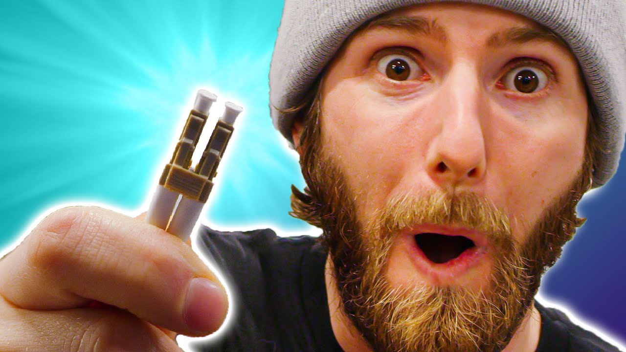
- 🛠️ 制作狭缝使用了旧的光刻掩模和光阻层,通过UV光曝光和铬层蚀刻。
- 🔄 使用了两种激光器进行实验:绿色激光二极管和红色氦氖激光器。
- 🔍 显微镜和相机的组合用于观察和记录实验结果。
Q & A
双缝实验是什么?
-双缝实验是一个经典的物理实验,用于展示光和其他粒子的波动性质。实验中,光波通过两个非常窄的缝隙,在另一端形成干涉图样,显示出亮暗条纹。
为什么视频作者认为有必要再次制作关于双缝实验的视频?
-作者认为大多数现有视频仅仅是讨论双缝实验,而不是真正展示实验过程。作者希望通过自己的版本,使用非常窄的缝隙和显微镜观察,来展示实验的更多细节。
作者使用的缝隙宽度是多少?
-作者制作的缝隙宽度从2.5到大约25微米不等。
在实验中,作者如何产生不同宽度的缝隙?
-作者使用旧的光刻掩模版和光阻层,通过紫外光按照缝隙的图案曝光,然后发展光阻并蚀刻下面的铬层,从而得到微小的透明缝隙。
作者在实验中使用了哪些激光器?
-作者在实验中使用了绿色激光二极管和红色氦氖激光器,两者都适用于实验,但氦氖激光器的光束质量通常更好。
实验中观察到的亮暗条纹是如何形成的?
-当光波通过两个窄缝隙后,它们在垂直于缝隙的方向上相互干涉,形成亮暗条纹。这些条纹是由于光波的相位差造成的干涉现象。
为什么单个缝隙的光强分布不是均匀的?
-这是因为在微观尺度上,光波通过单个缝隙时已经产生了干涉结构,当它开始与其他缝隙的光干涉时,就形成了非均匀的光强分布。
实验中如何测量干涉图样?
-实验中通过在显微镜的另一侧放置相机,相机的物镜将光投射到CMOS芯片上,从而捕获干涉图样。
作者为什么选择在显微镜下观察双缝实验?
-使用显微镜允许作者在更近的距离和更小的尺度上观察干涉现象,这样可以更详细地研究实验的各个方面。
实验中缝隙之间的距离是如何变化的?
-作者在实验中改变了缝隙之间的距离,以研究不同距离对干涉图样的影响。
实验结果与单个缝隙的光强度简单相加有何不同?
-实验结果显示,两个缝隙的光相互干涉形成的干涉图样与单个缝隙的光强度简单相加得到的图案有很大不同,干涉图样更为复杂且具有更多的细节。
Outlines
🌟 双缝实验介绍与独特版本展示
本段介绍了双缝实验的背景和视频制作的目的。虽然双缝实验已有200多年的历史,并且YouTube上已有大量相关视频,但大多数视频只是讨论而非展示实验本身。视频作者强调,他将展示自己版本的实验,使用比大多数实验更窄的光波长宽度的狭缝,并在显微镜下而非远距离屏幕上研究衍射现象,以便更详细地观察实验的各个方面。作者制作了从2.5到25微米不同宽度的狭缝,并在实验中改变了狭缝间的距离。视频首先展示了实验中实际观察到的现象,然后解释了实验的工作原理和图像的形成过程。
Mindmap
Keywords
💡双缝实验
💡光的波长
💡干涉
💡衍射
💡激光束
💡显微镜
💡光强度分布
💡光束质量
💡光刻
💡DIY掩模步进器
💡测量装置
💡CMOS芯片
Highlights
这个视频介绍了双缝实验,一个超过200年历史的实验。
大多数视频只是讨论双缝实验,而不是展示实验本身。
视频展示了作者自己的双缝实验版本,使用了非常窄的缝宽,仅几倍光波长。
实验在显微镜下进行,而不是在大屏幕上观察。
实验中使用了2.5到25微米不同宽度的缝隙。
实验还改变了缝隙之间的距离。
展示了激光束通过约3.5微米宽的两个非常窄缝隙后的强度分布。
观察到光在垂直于缝隙的方向上形成了明亮和黑暗的条纹。
单个缝隙的光并不是均匀扩散,而是在与其他缝隙的光视觉干涉之前就包含了很多干涉结构。
实验中观察到的干涉模式与仅将单个缝隙的强度相加得到的模式有很大不同。
实验使用的是真实的观测数据,而不是模拟结果。
为了制作实验用的缝隙,使用了旧的光刻照片掩模。
通过使用紫外光照射光刻层,并在缝隙的图案下曝光,来蚀刻出透明缝隙。
实验中使用了两种激光:绿色激光二极管和红色氦氖激光。
绿色激光通过小透镜准直后投射到蚀刻在显微镜载物台上的缝隙上。
红色氦氖激光通过分光镜直接向上引导至缝隙。
显微镜位于缝隙的另一侧,可以前后移动以观察缝隙图案。
显微镜的目标镜将光投射到相机的CMOS芯片上。
Transcripts
Hello everybody, This video it about the double slit experiment
and maybe you wonder why someone wants to make yet another video about a more than 200
years old experiment.
Especially with already tons of videos on YouTube regarding the subject.
Well, for one: most videos don't show the experiment, but just show you people talking
about it.
But in this video, we will have a look at the real deal.
And, because I show you my own version of the experiment, there is a good chance that
My version of the experiment uses slits that have a width in the order of only a few wavelengths
of light, which is actually significantly narrower than used in most experiments.
And we will study diffraction under a microscope instead of at a large distance on a screen.
This allows us to look at a few aspects of the experiment with much greater detail.
So, to perform the experiment, I made various slits ranging from 2.5 to about 25 microns.
And in the experiments, I also varied the distance between the slits.
So let me first show you what you actually see in the experiment, and after that, let's
have a look at how the experiment works and how the images were made.
Here we are looking at the cross section of a laser beam showing the intensity distribution.
This beam is sent through two very narrow slits of approximately 3.5 microns wide.
And this is what you observe after the light has passed the slits.
It spreads out, in these bright and dark bands, especially in the direction perpendicular
to the slit.
By the way, notice how the individual slits are not spreading the light as a uniform bump.
And this is because of the scale at which we're observing, Basically, everything you
see here happens within 1 cubic millimeter.
You can see that the pattern of an individual slit already contains a lot of interference
structure before its light starts to visually interfere with that of the other slit.
As we move further away, the light of the two slits gradually starts to interact.
Here at the bottom, you see an intensity profile plotted and this graph shows you the sum of
intensities of the pixel columns in a part of the image above the graph.
Now notice how the interference pattern develops between the slits, first there in the center,
and later spreads out over almost the complete extend of the pattern.
You can actually measure that the interference pattern is quite different from the patterns
you would get if you would just add up the intensities of the individual slits.
What you see here is all experimental and is not just some simulation.
And I wanted to show you this first, to demonstrate that the double slit experiment actually contains
way more fascinating details than are normally presented.
used old lithographic photomasks for this purpose.
To etch the patterns, I used a photoresist layer, and exposed this layer with UV-light
in the pattern of the slits.
After that, the photoresist was developed and chromium underneath was etched in the
desired pattern.
The result is tiny transparent slits in the chromium layer.
By the way, the exposure patterns in the photoresist were produced by using the DIY maskless wafer
stepper that featured in several of my previous videos.
And here is the measurement setup.
For the experiments I actually used 2 different lasers: a green laser diode and a red helium
neon laser.
They both worked fine.
However, generally the beam quality of the Helium Neon laser was a bit better.
When using the green laser, light was collimated with a small lens and then projected on the
slits, which were etched in this disk placed on the table of the microscope.
In the case of the HeNe-laser I just used a beam splitter to direct the beam upward
towards the slits.
On the other side of the slits is the microscope that can be moved from and to the slit pattern.
And the objective of the microscope projects the light on the CMOS chip of a camera, which
浏览更多相关视频
5.0 / 5 (0 votes)