MOSFET - Differential Amplifier (Small Signal Analysis)
Summary
TLDRThis video from the ALL ABOUT ELECTRONICS YouTube channel delves into the small signal analysis of a differential amplifier, focusing on determining its gain. The presenter explains that for linearity in the input-output relationship, the differential input should be small. Using small signal approximation, the video derives the differential gain formula as -gm * (Rd ∥ R0), considering the channel length modulation. An example illustrates the low gain of the amplifier and discusses limitations in increasing gain due to power consumption and supply voltage constraints. The video concludes with a teaser for the next episode, which will explore methods to enhance the differential amplifier's gain.
Takeaways
- 🔍 The video covers the small signal analysis of a differential amplifier, focusing on finding its gain.
- 📊 A previous video discussed large signal analysis, providing the operating range and relationship between differential input and output.
- 🎚️ For linear amplification, the differential input must be small to ensure a linear relationship between input and output.
- 🔧 The video explains the small signal approximation condition and how it simplifies the differential amplifier's analysis.
- 🔗 Small signal analysis treats DC sources and common mode inputs as zero, focusing on the differential components.
- 🛠️ The video replaces MOSFETs with their small signal models to analyze the circuit's behavior more easily.
- ⚖️ By using Kirchhoff's laws and assuming matched MOSFETs, the analysis is simplified, treating node x as a virtual ground.
- 📉 The differential gain of the amplifier is derived as -gm * Rd, showing the relationship between the output and input.
- 📏 Channel length modulation and its effect on the differential gain are considered, adjusting the gain formula to include output resistance.
- 📈 The video concludes by discussing ways to improve the gain, such as increasing the drain resistor or trans-conductance, while also acknowledging the limitations of these methods.
Q & A
What is the purpose of small signal analysis in the context of a differential amplifier?
-The purpose of small signal analysis is to linearize the relationship between the differential input and output of a differential amplifier. This allows for easier calculation of the amplifier's gain when the differential input is very small.
Why is the input voltage Vin1 - Vin2 considered to be small in small signal analysis?
-The input voltage Vin1 - Vin2 is considered small in small signal analysis because the relationship between the differential input and output is nonlinear for large inputs. To maintain a linear relationship and use the amplifier effectively, the differential input must be small.
How does the small signal approximation affect the current through the MOSFETs?
-Under the small signal approximation, the differential current (Id1 - Id2) simplifies, allowing us to neglect higher-order terms. This approximation makes it easier to analyze the circuit and find the small signal currents that contribute to the output.
What is the role of the transconductance (gm) in determining the gain of the differential amplifier?
-The transconductance (gm) is directly proportional to the differential gain of the amplifier. The differential gain is given by -gm * Rd, where gm represents the relationship between the gate-to-source voltage (Vgs) and the small signal drain current (Id).
Why can node X be treated as a virtual ground in the small signal analysis?
-Node X can be treated as a virtual ground because, under small signal conditions, the voltage at this node does not change due to the symmetry of the circuit and the matching of the two MOSFETs. This simplifies the analysis of the circuit.
What happens when the effect of channel length modulation is included in the small signal model?
-When the effect of channel length modulation is included, the output resistance of the MOSFET (R0) is introduced in parallel with Rd. This modifies the differential gain equation to -gm * (Rd ∥ R0), slightly reducing the gain.
What is the impact of increasing the drain resistor (Rd) on the differential gain?
-Increasing the drain resistor (Rd) increases the differential gain of the amplifier. However, this also increases the voltage drop across the resistor, potentially pushing the MOSFET out of saturation, which may require a higher supply voltage.
How can the transconductance (gm) be increased to improve the differential gain?
-The transconductance (gm) can be increased by increasing the bias current (Id) or the width-to-length ratio (W/L) of the MOSFET. However, increasing Id leads to higher power consumption, and increasing W/L results in a larger area occupied by the circuit.
What is the effect of increasing the bias current (Id) on the power consumption of the differential amplifier?
-Increasing the bias current (Id) increases the transconductance (gm), which improves the gain. However, this also increases the power consumption of the amplifier and may require a higher supply voltage to maintain MOSFET saturation.
Why is the differential gain of a typical differential amplifier considered low?
-The differential gain of a typical differential amplifier is considered low due to practical limitations in increasing the drain resistor (Rd), bias current (Id), and the width-to-length ratio (W/L). These factors restrict the achievable gain while maintaining reasonable power consumption and circuit area.
Outlines

此内容仅限付费用户访问。 请升级后访问。
立即升级Mindmap

此内容仅限付费用户访问。 请升级后访问。
立即升级Keywords

此内容仅限付费用户访问。 请升级后访问。
立即升级Highlights

此内容仅限付费用户访问。 请升级后访问。
立即升级Transcripts

此内容仅限付费用户访问。 请升级后访问。
立即升级浏览更多相关视频

Introduction to Operational Amplifier: Characteristics of Ideal Op-Amp
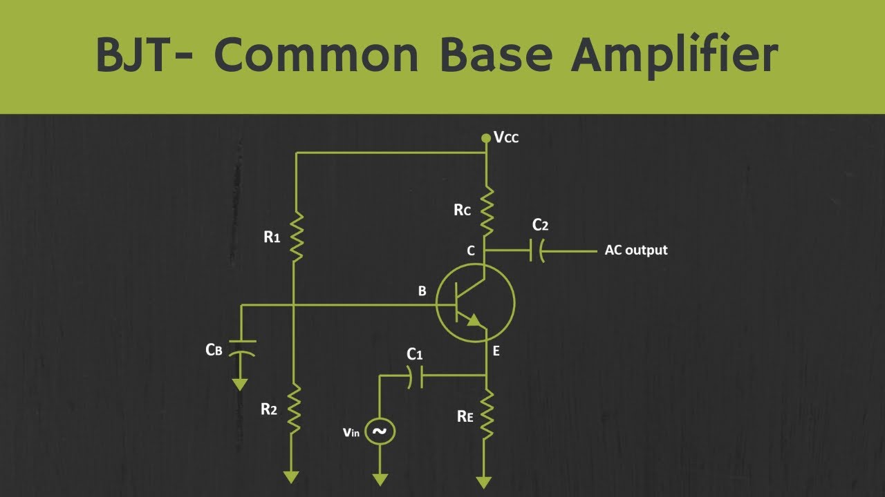
BJT- Common Base Amplifier Explained
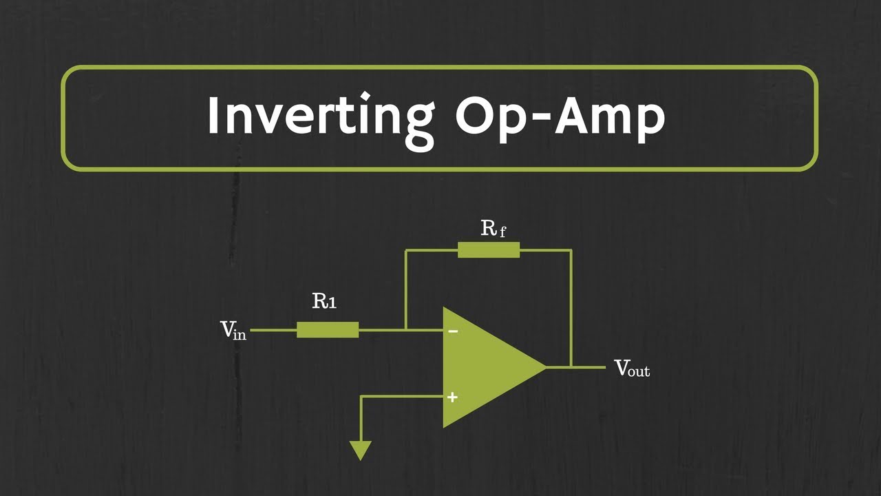
Operational Amplifier: Inverting Op Amp and The Concept of Virtual Ground in Op Amp

Small Signal Analysis of BJT
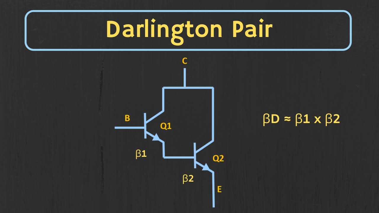
Darlington Pair Explained | The Darlington Pair as a Switch

How Oscillator Works ? The Working Principle of the Oscillator Explained
5.0 / 5 (0 votes)
