Silicon Photonics: The Next Silicon Revolution?

Asianometry
16 Jun 202215:45

Summary

TLDRSilicon Photonics is a revolutionary technology that merges silicon manufacturing with photonics for high-speed data transmission. It aims to replace copper wiring with optical fibers for faster, more efficient communication. Despite challenges like silicon's inability to emit light and the lack of a modulator, the industry has made strides with workarounds and innovations, finding its niche in data centers and LiDAR systems. However, it seeks a broader market to realize its full potential and avoid the pitfalls faced by MEMS technology.

Takeaways

  • 🌌 Silicon Photonics is a futuristic technology that involves the manipulation of light using silicon-based components, similar to how MEMS applies CMOS processes to the mechanical world.
  • 🚀 The term 'Photonics' refers to technologies that transmit and manipulate light, or photons, which is crucial for optical data transmission and has advantages over traditional electrical signals in terms of speed and heat generation.
  • 🔌 The shift to using light for long-distance communications in the 1990s revolutionized the industry, allowing for higher data volume transmissions through optical fibers.
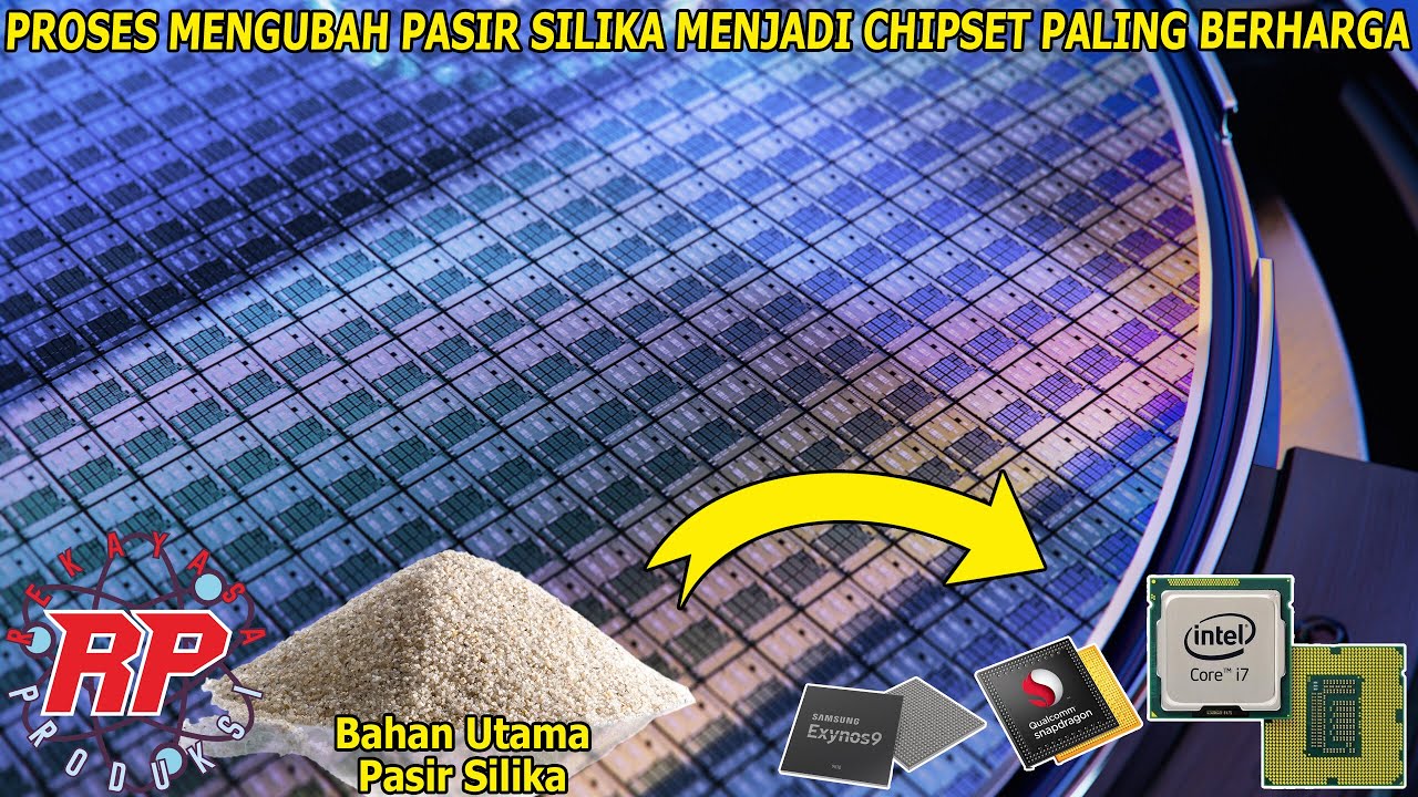
  • 🌐 Silicon is a key material in the electronics industry due to its abundance, low cost, and scalability, which has led engineers to explore its application in photonics.
  • 💡 The ideal silicon photonics system would consist of five components: a light source, pathways to manipulate light, modulators, photodetectors, and traditional CMOS electronics.
  • 🚧 Silicon's inability to emit light due to its indirect bandgap presents a significant challenge for creating a pure silicon light source, leading to the development of workarounds like external lasers or hybrid integration.
  • 🛠 Silicon modulators have seen steady progress, with Intel announcing a high-speed optical modulator in 2004 and a fully integrated CMOS silicon photonics transceiver in 2012.
  • 💼 The data center industry, particularly hyperscalers like AWS, Google, and Microsoft, has become a significant market for silicon photonics due to the need for high-speed, efficient data transmission within their vast server networks.
  • 🛰 The potential application of silicon photonics in LiDAR systems for autonomous vehicles offers the possibility of reducing costs and increasing resolution by integrating optical components onto a chip.
  • 🏭 Silicon photonics products require a specialized fabrication process using silicon-on-insulator (SOI) wafers, with companies like GlobalFoundries and Intel leading in this space.
  • 💡 The future of silicon photonics may lie in its ability to find a large and valuable commercial market, as it currently faces challenges in becoming mainstream due to competition with existing technologies and market size limitations.

Q & A

  • What is Silicon Photonics?

    -Silicon Photonics is a technology that applies modern nanoscale CMOS processes to the optical realm, enabling the transmission and manipulation of light, or photons, for high-speed data communication.

  • Why did networking companies switch from copper wires to optical fibers for data transmission?

    -Networking companies switched to optical fibers because light travels at the speed of light, allowing for super-high frequency transmissions and higher data volume. Optical fibers also avoid the slowdown and heat generation issues associated with electron movement in copper wires.

  • What are the benefits of using multiple light wavelengths in the same optical fiber?

    -Using multiple light wavelengths allows for the transmission of multiple signals through the same fiber without interference, greatly increasing the capacity for data transmission.

  • Why is silicon an attractive material for photonics applications?

    -Silicon is attractive due to its abundance, low cost, and the ability to scale manufacturing processes. It has been widely studied and used in the electronics industry, making it a candidate for integrating photonics with electronics.

  • What are the five components necessary for a monolithic silicon photonics chip?

    -The five components are: 1) A light source, usually a laser; 2) Passive structures for manipulating light; 3) A modulator to convert digital electronic signals to optical signals; 4) A photodetector to convert optical signals back to electronic signals; and 5) Traditional CMOS electronics for support functions.

  • What are the two main issues with integrating a light source into silicon photonics?

    -The two main issues are that silicon cannot emit light on its own due to its indirect bandgap, and it does not exhibit the Pockels effect, which is necessary for modulating light with electrical fields.

  • What is the significance of the development of silicon-based high-speed optical modulators?

    -The development of high-speed optical modulators, such as the one announced by Intel in 2004, marked a significant breakthrough, enabling the conversion of continuous laser light into digital signals, which is essential for data communication.

  • How does silicon photonics benefit data centers?

    -Silicon photonics can integrate transceiver functionality onto chips, replacing legacy components, which saves on cost, power, and labor, and addresses bandwidth bottlenecks in data centers.

  • What potential applications does silicon photonics have in the sensor and LiDAR markets?

    -Silicon photonics can potentially reduce the cost and size of LiDAR systems by integrating multiple optical components onto a chip, which is crucial for high-resolution, compact, and affordable sensors used in applications like autonomous driving.

  • What challenges does the silicon photonics industry face in terms of market adoption and integration?

    -The industry faces challenges such as finding large and valuable markets for its technology, as well as technical hurdles like the lack of a pure silicon-based laser and the difficulty of making photonics components smaller than the wavelength of light they use.

  • What is the current state of silicon photonics in terms of manufacturing and market presence?

    -Silicon photonics products are being manufactured using silicon-on-insulator wafers and are finding their niche in data centers and potentially in LiDAR and sensor markets. Companies like Intel, Cisco, and MACOM are selling millions of units annually, but the industry is still seeking broader mainstream adoption.

Outlines

00:00

🌌 Introduction to Silicon Photonics

The first paragraph introduces the concept of Silicon Photonics, a technology that applies nanoscale CMOS processes to the optical realm. It explains the shift from using electrical signals through copper wires to transmitting data via light through optical fibers, which is faster and more efficient. The paragraph also discusses the challenges of integrating photonics with silicon, including the need for a light source and modulator, and the limitations of silicon's inability to emit light natively.

05:03

🔍 The Silicon Optics Dream and Its Challenges

This paragraph delves into the aspirations of creating a monolithic silicon chip for photonics, which would include a light source, pathways for light manipulation, modulators, photodetectors, and traditional CMOS electronics. It highlights two main issues: silicon's inability to emit light due to its indirect bandgap and the lack of the Pockels effect, which is necessary for modulating light with electric fields. The paragraph also touches on the history of silicon photonics development and the workarounds used to overcome these challenges, such as external lasers and hybrid integration.

10:06

🚀 Advancements in Silicon Modulators and Data Center Applications

The third paragraph discusses the progress made in silicon modulators, from the announcement of Intel's high-speed optical modulator in 2004 to the development of fully integrated CMOS silicon photonics transceivers. It explains how these advancements have allowed the silicon photonics industry to move out of the laboratory and into commercial applications, particularly in data centers. The paragraph also introduces the concept of hyperscalers and how silicon photonics can improve internal data transmission performance, leading to significant cost, power, and bandwidth savings.

15:08

🛰️ LiDAR, Sensors, and the Future of Silicon Photonics

The final paragraph explores the potential of silicon photonics in the sensor and LiDAR markets, highlighting its ability to reduce costs and increase resolution for autonomous driving applications. It also discusses the manufacturing process of silicon photonics, the role of different fabs in the industry, and the challenges faced in finding large-scale commercial markets for this technology. The paragraph concludes by comparing silicon photonics to the MEMS industry and pondering its potential to become the next silicon revolution.

Mindmap

Keywords

💡Silicon Photonics

Silicon Photonics refers to the integration of photonics, the science of light, with silicon-based electronics to create devices that manipulate and transmit light. It is a key theme of the video, illustrating the potential of silicon to revolutionize optical communication and data transmission. The script discusses how silicon photonics can be used to overcome the limitations of traditional copper wire communications by leveraging the speed and efficiency of light.

💡Photonics

Photonics is the technology of generating, manipulating, and detecting light particles, or photons. It is central to the video's narrative, as it explains how photonics technologies are used for optical data transmission, which is faster and more efficient than traditional electrical signals. The script mentions that photonics involves the use of lasers, optical fibers, and various devices to manage light for communication.

💡MEMS

MEMS stands for Micro-Electro-Mechanical Systems, which are tiny devices that combine electrical and mechanical components at the micro-scale. The script uses MEMS as a comparison to explain how silicon photonics applies similar nanoscale CMOS processes to the optical realm, highlighting the innovation in miniaturizing and integrating systems.

💡Optical Fiber

Optical fiber is a thin strand of glass or plastic designed to transmit light signals over long distances. The video script emphasizes the role of optical fiber in revolutionizing long-distance communication by enabling the transmission of data at the speed of light, which is faster and more efficient than traditional copper wires.

💡Wavelength Division Multiplexing (WDM)

WDM is a method of transmitting multiple signals over the same optical fiber by using different light wavelengths. The script explains that WDM allows for increased data transmission capacity without the need for additional physical infrastructure, which is a significant advancement in optical communication technology.

💡Silicon Optics Dream

The Silicon Optics Dream refers to the aspiration to create a monolithic silicon chip capable of transmitting and manipulating light. The script discusses this concept as a driving force behind silicon photonics, aiming to combine the efficiency of silicon manufacturing with the capabilities of photonics.

💡Transceiver

A transceiver is a device that converts between digital optical signals and digital electronic signals. The script explains the importance of transceivers in data centers, where they facilitate the conversion of light data to electrical data, and vice versa, playing a crucial role in the integration of silicon photonics.

💡Indirect Bandgap

The indirect bandgap is a property of certain semiconductor materials, like silicon, where the energy states of electrons do not directly correspond to the emission of light. The script mentions this as a challenge for silicon photonics, as it prevents silicon from emitting light efficiently on its own, necessitating workarounds or modifications.

💡Pockels Effect

The Pockels effect is a phenomenon where an electric field can change the refractive index of a material, thus affecting the speed of light passing through it. The script explains that silicon's lack of the Pockels effect is a limitation for creating modulators, which are essential for converting digital electrical signals into digital light signals.

💡Mach-Zehnder Interferometer (MZI)

The MZI is a type of optical modulator that operates by splitting and recombining light waves to represent digital signals. The script highlights the significance of MZI in the development of silicon-based high-speed optical modulators, marking a milestone in silicon photonics technology.

💡Data Center

A data center is a large facility that houses computer systems and associated components, such as servers, storage devices, and network equipment. The script discusses how silicon photonics can be applied in data centers to improve internal performance and efficiency, particularly through the integration of transceiver functionality onto chips.

💡LiDAR

LiDAR, which stands for Light Detection and Ranging, is a remote sensing technology that uses light in the form of a pulsed laser to measure distances. The script explores the potential of silicon photonics to make LiDAR systems more affordable and compact, which is important for applications like autonomous driving.

💡Silicon-on-Insulator (SOI)

SOI is a type of semiconductor wafer with an insulating layer between the silicon device layer and the handle substrate. The script mentions SOI as the material used in silicon photonics products, which has special layers that help confine light, making it essential for the fabrication process of silicon photonics devices.

💡Hyperscaler

A hyperscaler refers to companies like Alibaba, AWS, Google, and Microsoft that offer massive cloud computing scalability. The script uses the term to describe the large-scale data centers these companies build, which are significant consumers of silicon photonics technology for internal data transmission.

Highlights

Silicon Photonics is an emerging technology that applies nanoscale CMOS processes to the optical realm.

Photonics technologies transmit and manipulate light, or photons, for optical data transmission.

Optical fiber communication is faster and more efficient than traditional copper wire due to the speed of light.

Wavelength division multiplexing allows multiple signals to be sent through the same fiber without interference.

Silicon is a widely studied and used element in electronics due to its abundance, low cost, and scalability.

Engineers aim to integrate CMOS manufacturing processes with photonics to create a monolithic silicon chip.

A complete photonics system requires five components: a light source, pathways, modulator, photodetector, and CMOS electronics.

Silicon's inability to emit light due to its indirect bandgap presents a significant challenge for silicon photonics.

Researchers have modified silicon to emit light, but commercial silicon-based lasers are not yet available.

Silicon's lack of the Pockels effect makes it difficult to create modulators for converting electrical signals to optical signals.

The development of silicon photonics began in the mid-1980s with the work of Richard Soref on adjusting silicon's refractive index.

Intel announced the first high-speed silicon-based optical modulator in 2004, using a Mach-Zehnder interferometer.

In 2012, Intel introduced a fully integrated CMOS silicon photonics transceiver with a ring modulator device.

Silicon photonics has found its first major commercial application in data centers, improving internal performance.

Hyperscalers like AWS, Google, and Microsoft are driving the demand for silicon photonics in data centers.

Silicon photonics has potential in the sensor and LiDAR markets, offering cost and size advantages.

Silicon photonics products use silicon-on-insulator wafers, requiring a specialized fabbing process.

GlobalFoundries and Intel are significant players in silicon photonics manufacturing, with TSMC focusing on integration schemes.

Silicon photonics faces challenges in finding a large and valuable commercial market to fulfill its potential.

The industry is exploring the use of silicon photonics in microprocessors to disrupt traditional semiconductors.

Silicon photonics is in search of a market that can capitalize on its futuristic technology and applications.

Transcripts

play00:03

Silicon Photonics. What a cool-sounding word.

play00:06

It sounds like something from  the age of the Jetsons. But  

play00:09

behind that futuristic phrase is a simple need.

play00:12

If MEMS is the result of applying modern  nanoscale CMOS processes to the mechanical world,  

play00:17

then doing the same for the optical  realm gives us Silicon photonics.

play00:22

In this video, I want to talk about  another magic silicon technology.  

play00:25

One that’s starting to make a splash  in the contemporary technology world.

play00:40

## Photonics

play00:47

Let us break it down - starting with "Photonics".

play00:50

Photonics. What does that mean?  Lasers? Sharks with lasers?  

play00:54

Eyeglasses? Lithography machines? How  does that jive with the silicon world?

play00:59

In the context I am talking about here, photonics  technologies transmit and manipulate light - in  

play01:04

the form of light particles or "photons". It is  related to the world of optical data transmission.

play01:10

Previously, networking companies  communicated using electrical signals sent  

play01:14

through copper wire. The issue is that  the electrons traveling through such  

play01:18

wires interact with other atoms, which  slows them down and generates heat.

play01:24

By the 1990s, networking companies found  themselves struggling to deal with exploding  

play01:28

data traffic network demands. They revolutionized  long distance communications by switching  

play01:33

to using light - sent via optical fiber - to  efficiently transmit data across great distances.

play01:40

Light moves through optical fiber at the speed of  light. Nothing is faster than the speed of light.

play01:45

This lets us transmit optical  signals at super-high frequencies,  

play01:49

which means higher data volume transmissions.  Later on, engineers took the concept yet  

play01:54

another step forward - sending multiple  signals through the same fiber by using  

play01:59

different light wavelengths that  won't interfere with each other.

play02:03

Today, optical fiber technologies dominate the  long-distance communications space. Over 2 billion  

play02:08

kilometers of optical fiber have been deployed,  enough to wrap around the world over 50,000 times.

play02:14

## The Silicon Optics Dream

play02:15

Now, silicon. The nano-electronics industry  has been using silicon for decades.  

play02:20

The element is the single most widely  studied element in human history.  

play02:24

It is plentiful, low-cost  and allows for massive scale.

play02:29

People have been able to make silicon do  amazing things - billions of transistors  

play02:33

on one wafer. Entire systems on chips that are  faster, smaller, and cheaper than their priors.

play02:41

And for that reason, engineers have wanted to  

play02:43

bring the titanic scale of modern  CMOS manufacturing - with its EDAs,  

play02:48

PDKs, and all the other tools and processes  used for it - over to the photonics world.

play02:53

Furthermore, transistors on traditional  chips right now are still communicating  

play02:58

using electrons through wires. What if you  were to replace those wires and electrons  

play03:03

with optical fibers and light? More on that later.

play03:06

## The Five Photonic Ingredients

play03:08

Dreams of a monolithic silicon chip -  meaning everything on it being made of  

play03:11

a single material system - transmitting and  manipulating light date back to the 1970s.  

play03:18

Such a system would have five components:

play03:21

One. A light source, usually a laser;

play03:24

Two. Routes and pathways to manipulate light.  Bend it, guide it, filter it, couple it,  

play03:30

split it, and combine it - kind of like optical  fiber does but just within the integrated chip.

play03:36

These are broadly referred  to as passive structures,  

play03:40

but as with legos there are different  shapes and structures with their own names;

play03:45

Three and Four. Ways to convert digital  electronic signals into digital optical  

play03:50

signals and vice versa. The former is  called a modulator, three. The latter  

play03:55

is a photodetector, four, which  makes sense if you think about it;

play03:59

A component that can do both  modulator and photodetector work  

play04:02

is called a transceiver. In data centers, a  transceiver sits at each end of the optical  

play04:08

cable, converting light data to  electrical data back and forth.

play04:12

And finally, number five, we need traditional CMOS  

play04:15

electronics to accompany the various  aforementioned photonics components.  

play04:20

These serve support functions like  encoding and decoding certain data items.

play04:25

Anyway. So there you have it,  a complete photonics system  

play04:28

that researchers are trying to incorporate all  onto a single monolithic chip. But there’s one  

play04:33

big issue. Actually, two. And they have to  do with the light source and the modulator.

play04:38

## The Two Issues

play04:39

The first is that, on its own, silicon cannot  emit light. Crystalline silicon has what is called  

play04:46

an indirect bandgap. This prevented it from  being used for the first Light Emitting Diodes  

play04:52

or LEDs and also means that it cannot lase.

play04:56

Without lasing, we cannot use silicon to  make light. No pure silicon light source.

play05:02

Researchers and engineers have to modify the  silicon structure to force it to emit light. For  

play05:08

instance, they implanted boron into the silicon  to finally create efficient, room-temperature  

play05:13

silicon-based LEDs. But commercial  silicon-based lasers still aren't there yet.

play05:20

Second, silicon's crystal structure means  that it does not exhibit the Pockels effect.  

play05:25

The Pockels effect describes a phenomenon  where you can use an electric field to  

play05:29

control how fast light goes through a certain  object. In other words, its refractive index.

play05:36

Lasers typically lase continuously.  The modulator's purpose is to convert  

play05:41

its continuous lasing into a digital  signal. The preferred way to do this  

play05:45

is with a material sitting in front of the  light, changing its intensity by absorbing it.

play05:51

If we cannot control light's progress  through silicon using electrical fields  

play05:55

then we cannot convert digital electrical  signals into digital light signals. No modulator.

play06:01

These two big issues make it that much harder  to produce a fully-integrated photonics device  

play06:07

out of pure silicon using the same  methods we use to make an Apple A15,  

play06:11

Intel Core, or MEMS accelerometer part.

play06:15

Early optics researchers instead focused on other  

play06:18

materials and made a great deal of progress  with gallium arsenide and indium phosphide.

play06:24

## Development

play06:25

Silicon photonics as we know it  today starts in the mid-1980s  

play06:29

with the work of Richard Soref. In 1987,  he co-authored a paper discussing how  

play06:34

silicon can be manipulated into  adjusting its refractive index.

play06:38

From there, the industry was able  to replicate one of the elementary  

play06:42

building blocks of a semiconductor  electronic devices - called a P-N  

play06:46

junction - using a type of photonic  passive structure called a waveguide.

play06:52

This kickstarted the silicon photonics  industry, which began work on building  

play06:56

out a photonics system with a  practical light source and modulator.

play07:01

The light source is where silicon  faces its greatest challenge.  

play07:04

Scientists have tried a lot of  things in order to make it lase.

play07:08

A silicon-based laser is considered the "Holy  Grail" of the silicon photonics space - the  

play07:13

final piece of the puzzle. But with that still  far off, engineers settled on workarounds.

play07:19

The most pragmatic workaround is to use an  external laser positioned outside the chip itself.  

play07:25

This has the added benefit of keeping  the chip from getting overheated.

play07:29

Another is to bond a pre-made laser  made from a different material like  

play07:34

Indium phosphide - something  known as hybrid integration.  

play07:37

Today, most commercial silicon  photonics providers do one of the two.

play07:41

## The Modulator

play07:43

Silicon modulators had been studied from the very  beginning, with slow but steady breakthroughs  

play07:47

throughout the 1980s and 1990s. First in shrinking  the device and then in speeding up its throughput.

play07:55

In 2004, Intel announced the first silicon-based  high-speed optical modulator, meaning to have a  

play08:00

bandwidth over 1 gigahertz. This attracted huge  media attention and represents a big breakthrough.

play08:07

That 2004 system used a Mach-Zehnder  interferometer - shortened to MZI.

play08:13

These modulators work by splitting light into two  

play08:16

wavelengths and then recombining  them to replicate a 1 or 0 signal.

play08:20

Then in 2012, Intel announced their first fully  integrated CMOS silicon photonics transceiver  

play08:27

with four channels, each at 25 Gigabit per  second. It was fabbed with a 90 nanometer process.

play08:34

This used a different type of modulator - a ring  

play08:36

modulator device that offers  size benefits over the MZI.

play08:41

With these advancements, the silicon  photonics industry managed to progress  

play08:45

out of the laboratory despite still lacking a  pure silicon-based laser. The industry quickly  

play08:51

found its first big commercialization  opportunity inside the data center.

play08:54

## The Data Center

play08:57

A "Hyperscaler" is a term  that describes Alibaba, AWS,  

play09:00

Google and Microsoft - companies offering immense  cloud computing scalability to their customers.

play09:07

To do this, they are building out  titanic data centers - spending  

play09:11

tens of billions a year in capital expenditure.

play09:14

There is more data transmitting between a couple  hundred servers within a single hyperscaler data  

play09:19

center than what goes between the east and west  halves of the United States public internet.  

play09:24

Thus the hyperscalers are always looking for  new ways to improve their internal performance.

play09:30

If you might recall from earlier, transceivers are  

play09:32

products that convert between digital  optical and digital electrical signals.

play09:36

They are a separate item that is plugged into  the switchgear at the top of each server rack.  

play09:41

Data flows through optical fiber into  the servers through this equipment.

play09:46

With silicon photonics you can now  integrate transceiver functionality  

play09:49

right onto the chip - replacing the legacy  component. Using them saves on cost,  

play09:55

power, and labor and cracks  a bandwidth bottleneck.

play09:59

Today, companies like Intel, Cisco, and MACOM are  selling millions of units a year. And photonic  

play10:05

components will continue to take share from legacy  optics and copper wire in this expanding space.

play10:11

## LiDAR and Sensors

play10:12

Silicon photonics's biggest market in the  short term will likely be in the data center.  

play10:16

But there is some potential in  the sensor and LIDAR markets.

play10:21

LiDAR uses light to help acquire a 3-D  picture of a particular environment.  

play10:26

As the name implies, it works similar to RADAR.  

play10:29

But since optical light waves are so much smaller  than radio waves, you can get higher resolutions.

play10:35

It is seen as an important part  of the autonomous driving puzzle.  

play10:39

The problem is that LiDAR setups are rather  expensive. Depending on what you are using,  

play10:44

a single system can cost up to $70,000. They  are also quite bulky, which has its own issues.

play10:51

A silicon photonics-based LiDAR system  offers the possibility of integrating  

play10:55

many discrete optical components right  onto the chip. This would drastically  

play10:59

bring down LiDAR costs in addition to  shrinking it to a more manageable size.

play11:04

There are a number of companies pursuing  this space. Intel subsidiary Mobileye  

play11:08

recently presented a small LiDAR  system on chip with integrated lasers.

play11:14

This is a pretty crowded space, with  notable other players including Pointcloud,  

play11:18

Aeva, Voyant Photonics, and Analog  Photonics. LiDARs are so hot right now.

play11:23

## Fabs

play11:25

Silicon photonics products use  silicon-on-insulator or SOI wafers.  

play11:29

These are wafers with special layers - usually  silicon dioxide - in addition to the silicon.  

play11:35

The layers' contrasting refractive  indices help confine light.

play11:40

Because of this, silicon photonics require a  slightly different fabbing process a couple  

play11:44

years behind the leading edge. This makes it  a speciality node with special opportunities  

play11:50

for foundries not looking to compete  for silly things like 3 nanometers.

play11:54

GlobalFoundries in particular has done a lot  in the space. They had acquired a great deal  

play11:58

of relevant IP from IBM when they acquired Big  Blue's Microelectronics division back in 2014.

play12:05

Dylan Patel of SemiAnalysis - which I recommend -  seems to believe that they are the market leader.  

play12:11

It's great for them after they abandoned  going for the leading edge a few years back.

play12:16

Intel has been an R&D pioneer for  silicon photonics for a very long time.  

play12:21

They are also setting up a foundry and  I feel that they would be missing out  

play12:24

if they didn't offer some of that  IP and capability to outsiders.

play12:28

And finally, TSMC. They have  not offered much in this space,  

play12:32

an absence that more than a few have noticed.

play12:35

Recently, it seems like their corporate strategy  has been building up integration schemes that  

play12:39

allow silicon photonics chiplets to work together  seamlessly with traditional semiconductors.

play12:45

I’ve been wondering about this for a while  and here’s my thinking. The issue seems to  

play12:49

be one of volume. The single biggest market  is transceivers. A market research publication  

play12:54

estimates about 50-75 million transceiver  units sold annually over the next few years.

play13:00

Assuming a 200 millimeter SOI wafer,  

play13:03

a 25 millimeter die, and 100% yield then that's  about 40-60,000 wafers for an entire industry.  

play13:11

Less than a month's production for a typical  mega-fab. Broken down to any one customer,  

play13:16

that's just a few days' run at a foundry. I guess  for TSMC, the juice isn’t worth the squeeze.

play13:22

## The Next Silicon Revolution?

play13:23

It illustrates one of the challenges  the industry now faces. Even if it takes  

play13:28

over the entirety of the transceiver and LiDAR  markets, what other big markets are out there?

play13:34

Investors and enterprises have poured hundreds  of millions of dollars into silicon photonics  

play13:39

R&D over the years. And it's yielded some  fruits but not enough to go mainstream.

play13:45

Thus some startups have sought to achieve  the dream of the 1970s. Replacing the copper  

play13:51

wiring on chips with optical fiber to create  a silicon photonics microprocessor capable of  

play13:56

disrupting traditional semiconductors.  But there are challenges here too.

play14:02

Today's leading edge transistors now have feature  sizes only a few nanometers large. But photonics  

play14:08

components cannot be made smaller than the  wavelengths of the light they carry. This tops  

play14:12

out at about 1 micrometer. Electrons on the other  hand, have wavelengths of just a few nanometers.

play14:19

At the 7 nanometer node, 1 square micrometer  of real estate can house over a hundred  

play14:25

transistors - a very high opportunity cost. It  pushes the industry away from highly-integrated  

play14:31

silicon photonics monoliths and towards  packaging solutions that pair photonics  

play14:36

and traditional chiplets together. Which  might explain what TSMC is doing right now.

play14:42

It's not a dealbreaker. Like I said,  

play14:43

there are a few startups out there working  on it. But it is something to think about.

play14:47

## Conclusion

play14:48

I discussed in an earlier video the  situation faced by the MEMS industry.  

play14:53

That industry sells millions of  units each year for everyday items  

play14:56

like accelerometers and sensors.  Units-wise, it’s a legitimate hit.

play15:01

However, each MEMS die sells for cents - with  the majority of value accruing to the packaging.  

play15:08

This has stifled innovation and made MEMS  commercialization extremely difficult.  

play15:13

As a result, the technology has yet  to really hit its financial potential  

play15:17

as the next silicon revolution.

play15:20

Silicon photonics is a technology from the future,  vying to change the way things are done. But it  

play15:26

also happens to be a technology in search of  a commercial market big and valuable enough to  

play15:31

fulfill its potential. Without that, it risks  suffering the same fate as its elder sibling.

Rate This

5.0 / 5 (0 votes)

Related Tags
Silicon PhotonicsOptical FiberData CentersLight TechnologyMEMSTransceiversLiDARNanoscale CMOSInnovationTech RevolutionIndustry Analysis