Packaging Part 16 1 - Overview of Silicon Photonics
Summary
TLDRDaniel Nguyen's video discusses silicon photonics, a technology leveraging light for faster data transmission than electronics. It covers the industry's supply chain, components like waveguides and modulators, and fabrication processes. The video also explores packaging complexities, integration methods, and challenges unique to photonic integrated circuits (PICs) compared to electronic integrated circuits (EICs).
Takeaways
- 🌟 Silicon photonics (SiPh) is a technology that uses light (photons) instead of electricity to process and transmit information, offering faster data transmission speeds.
- 🏭 Silicon is a cheap, abundant metalloid that can be easily integrated with current electronics, making SiPh a promising field with applications in communications, data processing, quantum computing, and more.
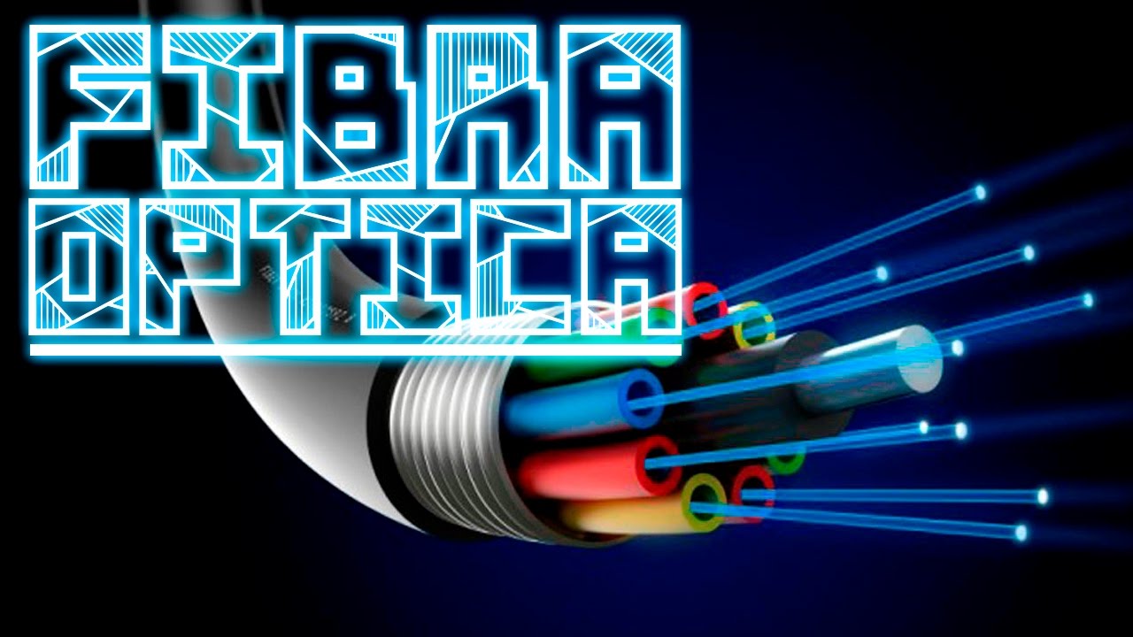
- 📡 Optical fibers are a key medium for transmitting data using SiPh, showcasing the practical application of photonics.
- 🔗 Companies like Intel, Nokia, Raytheon Technologies, and Cisco are investing in SiPh, indicating its potential for broad industry adoption.
- 🏢 The SiPh supply chain includes designers, substrate manufacturers, epitaxial manufacturers, foundries, and system integrators, highlighting the complexity of the industry.
- 🧩 Key components of SiPh include waveguides, modulators, detectors, optical couplers, lasers, optical fibers, and photodiodes, each playing a critical role in the technology.
- 🛠️ Packaging SiPh components can be complex due to the need for optical, electrical, thermal, and mechanical integration, requiring specialized techniques.
- 🔧 The fabrication process of SiPh involves wafer manufacturing, lithography, etching, doping, and selective epitaxial deposition, followed by back-end processing.
- 💻 The design flow for SiPh includes system specification, design, verification, and testing, often requiring iteration between physical and behavioral levels.
- 🔄 Integration of SiPh with electronic circuits can be achieved through various methods like wire bonding, interposer, flip chip, 3D stacking, and monolithic integration, each with its own advantages and challenges.
- 🚀 Monolithic integration offers the highest efficiency but is also the most complex and costly, suggesting a trade-off between performance and practicality in SiPh integration.
Q & A
What is Silicon Photonics?
-Silicon Photonics, or SiPh, refers to silicon-based technologies that use light (photons) to process and transmit information instead of electricity, which is what traditional electronics use.
Why is silicon used in Silicon Photonics?
-Silicon is used because it is a cheap, abundant metalloid that can be easily integrated with current product technology due to its semiconductor properties.
How is Silicon Photonics different from traditional electronics?
-Silicon Photonics uses photons, which travel at the speed of light, to transmit data, potentially offering faster data transmission speeds compared to the speed of electrons in traditional electronics.
What are some applications of Silicon Photonics?
-Silicon Photonics can be used to improve communications, data processing, quantum computing, medical imaging devices like OCT machines, and enhance data transmission speeds for virtual reality and augmented reality.
Which industries are involved in the development of Silicon Photonics?
-Industries involved include chipmakers like Intel, telecommunications companies like Nokia, aerospace and defense companies like Raytheon Technologies, healthcare industry leaders like Heidelberg Engineering, and data center companies like Cisco.
What are the main components of Silicon Photonics integrated circuits?
-The main components include the silicon substrate, waveguides, modulators, detectors, optical couplers, lasers, optical fibers, optical ring resonators, and photodiodes.
What is the role of waveguides in Silicon Photonics?
-Waveguides are key components that guide light within the silicon substrate and are typically made of a material with a higher refractive index than the surrounding medium.
How do modulators function in Silicon Photonics?
-Modulators in Silicon Photonics are used to manipulate light waves to change their properties, such as phase, amplitude, or frequency.
What are the challenges in packaging Silicon Photonics?
-Packaging challenges include the need for a wide range of packaging technologies to produce functional modules, managing thermal issues, and the complexity of integrating photonic and electronic components.
What is the fabrication process for Silicon Photonics?
-The fabrication process includes wafer manufacturing, lithography and etching, doping with phosphorus and boron, selective epitaxial deposition of germanium, and back-end-of-line stack formation.
What are the different approaches to integrating Silicon Photonics with electronics?
-The approaches include wire bonding, interposer, flip chip, 3D stacking, and monolithic front-end integration, each with its own advantages and complexities.
How does Silicon Photonics design flow differ from traditional electronic design automation?
-The design flow for Silicon Photonics starts with system specifications and designs that progress to physical layout, followed by verification and testing, often requiring iterations between physical and behavioral levels or back to earlier stages for component optimization.
Outlines

This section is available to paid users only. Please upgrade to access this part.
Upgrade NowMindmap

This section is available to paid users only. Please upgrade to access this part.
Upgrade NowKeywords

This section is available to paid users only. Please upgrade to access this part.
Upgrade NowHighlights

This section is available to paid users only. Please upgrade to access this part.
Upgrade NowTranscripts

This section is available to paid users only. Please upgrade to access this part.
Upgrade NowBrowse More Related Video

Silicon Photonics: The Next Silicon Revolution?

What Is Optical Computing | Photonic Computing Explained (Light Speed Computing)

Moore's Law is Dead — Welcome to Light Speed Computers

1.1 - Semiconductor Industry: Present & Future (Kevin Zhang)

How Fiber Optics Works 🌎

Fibra óptica - ¿Qué es? ¿Cómo funciona?
5.0 / 5 (0 votes)