CMOS Fabrication Process | CMOS Fabrication Algorithm | CMOS Fabrication Process Steps
Summary
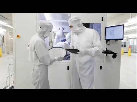
TLDRIn this detailed lecture, Professor Ritesh Kohler explains various fabrication processes, particularly focusing on the creation of metal oxide semiconductor materials and their applications in electronics. The lecture covers topics such as thermal oxidation, photolithography, and the importance of substrate types. The importance of precision in the fabrication process is emphasized, alongside the role of different materials and techniques like silicon, photolithography, and oxidation layers. The video concludes with practical insights into the challenges and methodologies of modern semiconductor fabrication, offering a deep dive into the world of material science and its applications.
Takeaways
- 😀 Understanding fabrication processes for semiconductor materials is crucial for modern technology development.
- 😀 The importance of metal oxide structures in semiconductor fabrication is emphasized, with particular focus on their application in electronic devices.
- 😀 Thermal oxidation is a key step in the creation of thin oxide layers in semiconductor fabrication.
- 😀 The process of photolithography is used to define patterns on substrates during fabrication, playing a major role in the development of transistors.
- 😀 Sourcing materials with proper semiconductor properties is essential for creating effective devices, such as the SiO2 layer.
- 😀 The integration of soft materials and layers helps in achieving desired electrical properties in semiconductor devices.
- 😀 Fabrication steps include oxidation, deposition, and patterning, which are followed by testing to ensure quality.
- 😀 The role of different substrate types, such as p-type and n-type, is vital in understanding the performance and behavior of semiconductors.
- 😀 Proper planning and structuring of fabrication processes are necessary for producing reliable and efficient components for modern electronics.
- 😀 Understanding the fabrication steps, from initial material selection to final application, provides insight into the complex world of semiconductor manufacturing.
Q & A
What is the primary focus of the lecture in the script?
-The primary focus of the lecture is to explain various fabrication processes, specifically in semiconductor manufacturing, involving materials like metal oxides and the steps in fabrication such as oxidation, photolithography, and the creation of thin oxide layers.
What role does oxidation play in the fabrication process?
-Oxidation is a crucial step in the fabrication process, as it helps in the creation of a thin oxide layer on the semiconductor substrate, which is vital for insulation and forming the basis for further processing, like photolithography.
What is the significance of photolithography in semiconductor fabrication?
-Photolithography is used to create patterns on the surface of a semiconductor material. It helps in defining the structure of the transistor and other components by transferring a pattern onto the material using light, typically ultraviolet.
How does the script explain the concept of substrates in semiconductor fabrication?
-The script discusses the importance of substrates, which are the foundational materials onto which other layers are built. The choice of substrate material impacts the quality and functionality of the final semiconductor device.
What is the importance of the 'thin oxide layer' mentioned in the script?
-The thin oxide layer is essential for insulation and electrical isolation in semiconductor devices. It plays a role in forming the gate oxide in transistors, which is critical for controlling the flow of current in the device.
What materials are mentioned as essential in semiconductor fabrication?
-Materials like silicon dioxide (SiO2), metal oxides, and photolithographic materials are mentioned. These materials are used to create thin insulating layers and patterns that define the electrical properties of the semiconductor devices.
What does the script refer to when discussing 'thermal oxidation'?
-Thermal oxidation refers to the process of growing an oxide layer on a semiconductor substrate by exposing it to an oxygen-containing environment at high temperatures. This process is vital for creating the insulating oxide layer needed in semiconductor devices.
How does the script describe the fabrication process involving photolithography and silicon dioxide?
-The script explains that photolithography is used to create patterns on the silicon dioxide (SiO2) layer. This process helps in defining the structures needed for transistors and other semiconductor components.
What is the role of 'subscribers' mentioned in the script?
-In the context of the script, 'subscribers' seems to refer to the users or followers who engage with the educational content, providing feedback or suggestions to improve the learning experience in future lectures.
What final step in semiconductor fabrication is mentioned in the script?
-The final step discussed involves the integration of various layers, including metal contacts and photolithographically defined patterns, to complete the semiconductor device, followed by testing and analysis of its functionality.
Outlines

This section is available to paid users only. Please upgrade to access this part.
Upgrade NowMindmap

This section is available to paid users only. Please upgrade to access this part.
Upgrade NowKeywords

This section is available to paid users only. Please upgrade to access this part.
Upgrade NowHighlights

This section is available to paid users only. Please upgrade to access this part.
Upgrade NowTranscripts

This section is available to paid users only. Please upgrade to access this part.
Upgrade NowBrowse More Related Video


5.0 / 5 (0 votes)