D Flip-Flop Explained | Truth Table and Excitation Table of D Flip-Flop
Summary
TLDRIn this video, the D Flip-Flop is introduced as a solution to the SR Flip-Flop's limitations. The script explains how the D Flip-Flop works by ensuring that both inputs are not 1 at the same time, allowing it to function as a reliable sequential circuit element. The video covers the Flip-Flop's behavior during clock transitions, its truth table, characteristic equation, and excitation table. It also highlights the internal circuitry, including the D latch and gated D latch, and how these are modified to create the D Flip-Flop. Finally, the video emphasizes its applications in data registers and counters.
Takeaways
- 😀 The D Flip-Flop solves the issue in the SR Flip-Flop by ensuring that both S and R inputs are not 1 at the same time.
- 😀 The D input is connected directly to the S input and through a NOT gate to the R input, creating a simple solution to prevent invalid states.
- 😀 When there is no clock transition, the D Flip-Flop holds its current state, meaning the output remains the same as the previous state.
- 😀 At a clock transition, the output of the D Flip-Flop follows the D input, either becoming 0 or 1, regardless of the previous state.
- 😀 The positive edge-triggered D Flip-Flop responds to the rising edge of the clock, while the negative edge-triggered version responds to the falling edge.
- 😀 The truth table for the D Flip-Flop indicates that it copies the input (D) at the clock transition, either setting the output to 0 or 1.
- 😀 The D Flip-Flop is widely used in digital circuits like data registers and counters, thanks to its predictable behavior.
- 😀 The Excitation Table is useful for designing digital circuits, showing the required input (D) to achieve a desired next state (Qn+1).
- 😀 The Characteristic Equation of the D Flip-Flop shows that Qn+1 = D, indicating that the next state is always equal to the current D input.
- 😀 The internal circuit of the D Flip-Flop can be derived from a basic SR latch, which is modified to create the D latch and then further adjusted to form the D Flip-Flop.
- 😀 The gated D latch can be converted into a D Flip-Flop by adding a clock transition circuit, which ensures the flip-flop responds only at the correct clock edge.
Q & A
What problem does the D Flip-Flop solve that the SR Flip-Flop cannot?
-The D Flip-Flop solves the issue of unpredictable output when both the Set (S) and Reset (R) inputs of the SR Flip-Flop are 1 simultaneously. This situation makes the SR Flip-Flop unreliable, but the D Flip-Flop ensures that S and R are never both 1 at the same time.
How does the D Flip-Flop ensure that both Set and Reset are not 1 at the same time?
-In the D Flip-Flop, the D input is connected directly to the Set (S) input, and the same D input is inverted and connected to the Reset (R) input via a NOT gate. This setup ensures that when D is 1, S is 1 and R is 0, and when D is 0, S is 0 and R is 1.
What is the primary function of a D Flip-Flop in sequential circuits?
-The primary function of the D Flip-Flop is to store data. It stores the state of its input (D) at the clock transition and holds that state until the next clock pulse, making it useful in registers and counters.
How does the D Flip-Flop behave when there is no clock transition?
-When there is no clock transition, the D Flip-Flop holds its current state. The output remains the same regardless of the value of the D input until the next clock pulse.
What happens to the output of the D Flip-Flop when D is 0 at the clock transition?
-When D is 0 at the clock transition, the output of the D Flip-Flop is reset to 0, regardless of its previous state.
What happens to the output of the D Flip-Flop when D is 1 at the clock transition?
-When D is 1 at the clock transition, the output of the D Flip-Flop is set to 1, regardless of its previous state.
What is the difference between a positive edge-triggered and negative edge-triggered D Flip-Flop?
-A positive edge-triggered D Flip-Flop responds to the rising edge of the clock signal to change its state, while a negative edge-triggered D Flip-Flop responds to the falling edge of the clock signal.
How does the output of a positive edge-triggered D Flip-Flop behave in a timing diagram?
-In a positive edge-triggered D Flip-Flop, the output follows the D input at each rising edge of the clock. The output remains in the same state between clock transitions, even if the D input changes.
What does the characteristic equation of a D Flip-Flop represent?
-The characteristic equation of a D Flip-Flop represents the relationship between the present state (Qn) and the next state (Qn+1) based on the D input. For the D Flip-Flop, the characteristic equation is Qn+1 = D, meaning the output always follows the D input.
What is the purpose of the Excitation Table in the context of a D Flip-Flop?
-The Excitation Table is used to determine the required input (D) for a D Flip-Flop to transition from one state (Qn) to another (Qn+1). It helps during the design and synthesis of digital circuits by indicating what input is needed for a desired output state.
Outlines

This section is available to paid users only. Please upgrade to access this part.
Upgrade NowMindmap

This section is available to paid users only. Please upgrade to access this part.
Upgrade NowKeywords

This section is available to paid users only. Please upgrade to access this part.
Upgrade NowHighlights

This section is available to paid users only. Please upgrade to access this part.
Upgrade NowTranscripts

This section is available to paid users only. Please upgrade to access this part.
Upgrade NowBrowse More Related Video

Penjelasan D Flip Flop

SR Flip Flop to JK Flip Flop Conversion

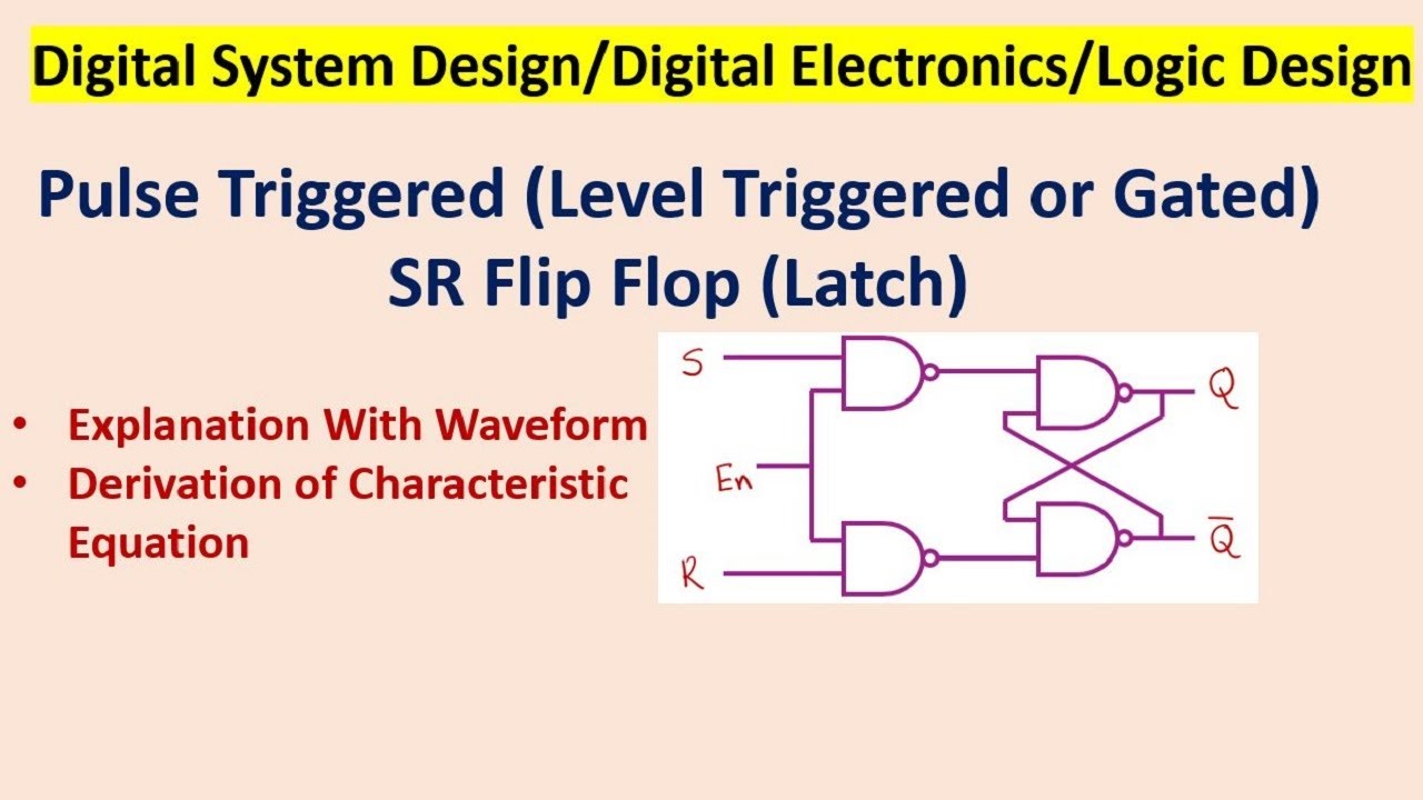
Pulse Triggered (Level Triggered or Gated) SR Flip Flop (Latch)

FLIP-FLOP - Jenis dan tabel kebenaran

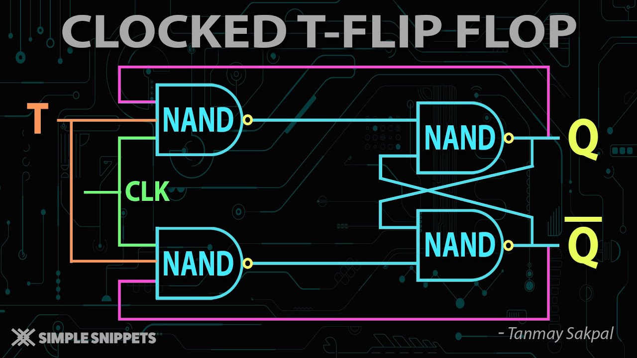
Clocked T Flip Flop using NAND Gates with Truth Table and Circuit Diagram

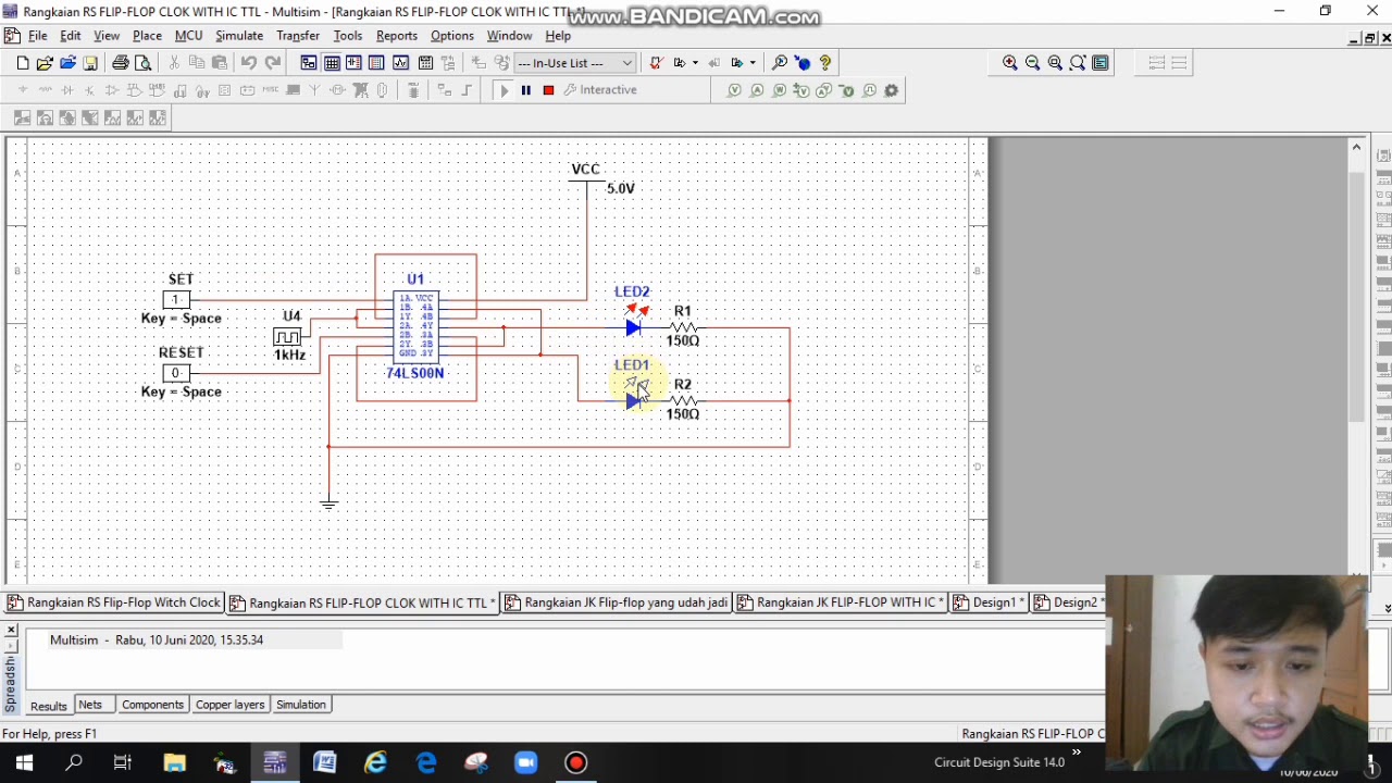
Simulasi Rangkaian JK Flip-flop, RS Flip-flop, dan D Flip-flop ( Faishal Satria G 2211181006 )
5.0 / 5 (0 votes)