(Nanorush 2024) How LEDs are Made : The Journey from Start to Bright!
Summary
TLDRDrin Abdullah, a scientist at the Institute of Nano-Opto Electronics Research and Technology at University Science Malaysia, discusses the fascinating world of LEDs (Light Emitting Diodes). He explains how LEDs are used in everyday devices and how they are more energy-efficient compared to traditional lighting. He delves into the structure, composition, and fabrication process of LED chips, focusing on materials like gallium nitride, and their role in generating blue light. The process involves intricate steps like deposition, photolithography, and etching, all aimed at creating efficient light sources for a sustainable future.
Takeaways
- π‘ LED technology is essential in daily life, powering devices like smartphones, laptops, smartwatches, and even cars.
- π About 25% of the world's electricity is used for lighting, making energy-efficient lighting technologies, like LEDs, critical.
- π¦ LEDs have various applications, from home lighting to public transport, traffic lights, entertainment, and even indoor gardening.
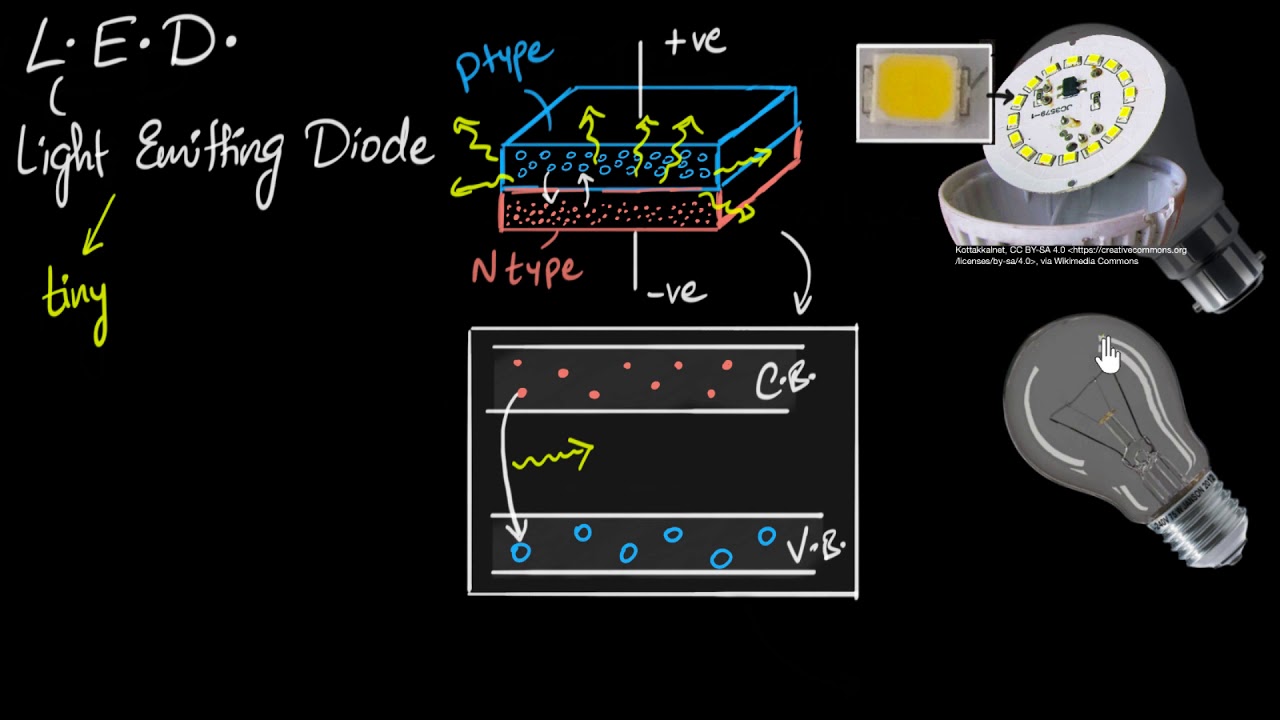
- π¨ The yellow square components inside an LED bulb are LEDs, with the yellow phosphor layer converting blue light into white light.
- π΅ Many white LEDs actually emit blue light, which is then transformed into white light by the phosphor layer on top.
- π The structure of an LED is made up of multiple layers, including metals and semiconductors like gallium nitride, which emits blue light.
- π¬ Gallium nitride layers can be adjusted to emit different colors of light, including green and ultraviolet, by modifying the indium content.
- π LED production involves a complex fabrication process, including wafer growth, metal deposition, photolithography, and etching.
- π Precise control of layer thickness, temperature, and materials is essential for producing high-quality LED chips with efficient light output.
- π In 2023, the institute developed a highly efficient white LED that exceeded industry standards, producing over 200 lumens per watt.
Q & A
What is Dr. Drin Abdullah's research focus?
-Dr. Drin Abdullah's research focuses on optics and photonics, with a specific interest in photonic devices such as light-emitting diodes (LEDs).
How much of the world's electricity is used for lighting?
-About a quarter of the world's electricity is used for lighting, which is a significant portion of global energy consumption.
What are some common applications of LEDs mentioned in the talk?
-LEDs are used in lighting homes, streets, car headlights, public transport, traffic lights, stage lighting for entertainment and sports, and even as artificial sunlight for growing vegetables indoors.
What is the primary component inside an LED bulb that produces light?
-The primary component inside an LED bulb that produces light is the LED chip, which is often made from a synthetic semiconductor material like gallium nitride (GaN).
How does the phosphor layer in an LED bulb contribute to the light production?
-The phosphor layer absorbs blue light emitted by the LED chip and converts it into yellowish light. The combination of blue and yellow light creates the white light we see.
What are the two common types of LED packages mentioned?
-The two common types of LED packages mentioned are SMD LEDs (Surface Mount Device) and DIP LEDs (Dual In-Line Package).
What is the role of the multiquantum well (MQW) layer in an LED?
-The MQW layer is the region where positive and negative charge carriers recombine, efficiently producing light. The composition of the MQW layer determines the color of the emitted light.
What are some materials used in the electrodes of an LED chip?
-The electrodes of an LED chip are typically made from metals like chromium, nickel, gold, and titanium, which allow for the flow of charge in the LED chip.
What is the significance of the MOCVD process in LED manufacturing?
-The Metal Organic Chemical Vapor Deposition (MOCVD) process is crucial in growing high-quality semiconductor layers, such as gallium nitride (GaN), with precise thicknesses and compositions. This process is essential for producing efficient LEDs.
How do LEDs compare to traditional tungsten lamps in terms of efficiency?
-LEDs are much more efficient than tungsten lamps because they primarily produce light instead of heat. In contrast, tungsten lamps generate light by heating a filament, which results in a significant loss of energy as heat.
Outlines
π‘ Introduction to Drin Abdullah and the Importance of LEDs
Drin Abdullah, a scientist at the Institute of Nano, Opto Electronics Research and Technology, University Science Malaysia, introduces himself and his work in optics and photonics. He explains the widespread use of light-emitting diodes (LEDs) in everyday devices such as smartphones, laptops, and cars. Abdullah highlights the energy consumption from lighting, noting that about 25% of the world's electricity is used for lighting. He stresses the importance of efficient lighting technologies like LEDs in reducing energy costs and consumption.
π Applications of LEDs
Abdullah describes various LED applications, from lighting homes and streets to powering car headlamps and traffic lights. He also mentions LEDs used in entertainment and sports venues. Fascinatingly, LEDs are used as artificial light sources for growing indoor vegetables, showcasing their versatility. Abdullah emphasizes the need for energy-efficient technologies like LEDs to reduce the cost of lighting and energy consumption.
π§ Inside an LED Bulb
Abdullah takes a deeper look into the structure of an LED bulb. He explains that the plastic cap (diffuser) spreads light, and beneath it lies multiple yellow-colored square components, each representing an LED. The yellow material is called phosphor, which absorbs blue light and emits yellow light. This combination produces white light. He further explains that white LEDs are essentially blue LEDs with a phosphor layer and describes two common types of packaged LEDs: SMD (Surface Mount Device) and DIP (Dual In-line Package) LEDs.
π¬ Structure of an LED and Semiconductor Materials
This section explores the structure of LEDs and the materials involved in their design. Abdullah explains that LEDs consist of metal, semiconductor, and insulator materials. The chip design includes layers of gallium nitride (GaN), a synthetic semiconductor that emits blue light. By adding different elements like magnesium and silicon to the GaN layers, the LED can generate positive and negative charge carriers, enabling light emission. The multiquantum well (MQW) layers in the chip determine the color of light, which can be fine-tuned by adjusting indium composition.
βοΈ Comparison with Tungsten Lamps
Abdullah compares the efficiency of LEDs with traditional tungsten lamps. He explains that tungsten lamps generate light by passing current through a resistor (tungsten wire), which produces light as the wire heats up. However, most of the energy is wasted as heat, making tungsten lamps highly inefficient. In contrast, LEDs efficiently produce light through the recombination of charge carriers in the semiconductor layers.
ποΈ LED Fabrication Process: Overview
Abdullah introduces the complex fabrication process of LEDs in an advanced laboratory. The process begins with LED structure development using Metal Organic Chemical Vapor Deposition (MOCVD), where layers are grown on a substrate like a layered cake. He discusses the importance of precision in monitoring, temperature control, and purity of materials during the growth process. These factors ensure defect-free, high-quality semiconductor layers needed for efficient LEDs.
π§ͺ Deposition, Photolithography, and Etching Processes
This section delves into specific stages of LED fabrication. Abdullah describes the deposition process, where thin layers of materials are added to the GaN layer using electron beam evaporators. He also explains photolithography, a process that uses light-sensitive polymers to create patterns on the wafer. The etching process, which removes unwanted material to form the desired LED structure, is also introduced. These processes are critical in shaping and preparing the LED chip for further stages.
π¬ Advanced Etching and Electrode Creation
Abdullah continues the fabrication process by detailing how the LED wafer is etched using inductively coupled plasma (ICP) to expose specific areas for metal electrode deposition. He explains the creation of negative and positive electrodes for the LED and describes how precision is necessary in placing metal contacts using techniques like photolithography and deposition. These steps ensure the LED functions properly when voltage is applied.
π₯ Metalization and Finalization of the LED Chip
The final steps of LED fabrication involve metalization, where the deposited metal contacts are heated to improve electrical conductivity and enhance the interface quality between the metal and semiconductor layers. Abdullah explains that this process reduces contact resistance and improves the LED's overall performance and reliability. He concludes by showing a cross-section of a completed blue LED chip, which efficiently lights up when voltage is applied.
π Conclusion and Final Thoughts
In the final section, Abdullah summarizes the LED fabrication process and expresses hope that the audience has learned valuable insights about LED technology. He thanks the viewers and wishes them success in their future endeavors.
Mindmap
Keywords
π‘LED (Light Emitting Diode)
π‘Phosphor
π‘Gallium Nitride (GaN)
π‘Semiconductor
π‘P-Type and N-Type Layers
π‘Multiquantum Well (MQW) Layer
π‘Metal Organic Chemical Vapor Deposition (MOCVD)
π‘Deposition
π‘Photolithography
π‘Etching
Highlights
Introduction to Drin Abdullah, a scientist at the Institute of Nano, Opto Electronics Research and Technology at University Science Malaysia, working in optics and photonics with a focus on light-emitting diodes (LEDs).
Explanation of the widespread presence of LEDs in everyday devices such as smartphones, laptops, tablets, smartwatches, cars, and homes, and their importance in modern lighting.
Emphasis on the significant energy consumption of lighting, accounting for about a quarter of the worldβs electricity generation.
Overview of various applications of LEDs, including lighting for homes, streets, vehicles, public transport, traffic lights, and even indoor agriculture.
Understanding of LED bulb components, including the diffuser and the yellow-colored phosphor layer which absorbs and emits different colored lights.
Inside an LED bulb, the actual light source is the blue light emitted by the LED, which is then combined with yellow light from the phosphor layer to produce white light.
Two common types of LED packaging: surface-mount device (SMD) LEDs, used in LED bulbs, and dual-in-line (DIL) LEDs, commonly seen in laboratories and electrical shops.
The critical role of the LED chip, a tiny semiconductor, which is the actual source of light in LED bulbs, protected by a polymer dome.
Explanation of LED chip materials: a sapphire substrate, layers of gallium nitride (GaN), and the multiquantum well (MQW) layer, where light is produced through recombination of positive and negative charge carriers.
Tuning the indium composition in MQW layers to produce different light colors, from blue to ultraviolet, making the LED versatile in color emission.
Comparison between LED technology and traditional tungsten lamps, highlighting the inefficiency of tungsten lamps which primarily produce heat energy instead of light.
Detailed fabrication process of LED chips in an advanced lab, starting with the LED epitaxial wafer growth using Metal Organic Chemical Vapor Deposition (MOCVD).
Challenges in the MOCVD process, requiring precise temperature control, monitoring systems, and high-purity precursors to avoid defects in the layers.
Insight into the deposition process of thin layers on the GaN wafer using Electron Beam Evaporator, crucial for constructing the LED chipβs structure.
Explanation of the photolithography process, used to create patterns on the wafer, followed by etching to remove unwanted areas, helping to shape the LED.
Final steps in the LED fabrication process: adding metal electrodes using Electron Beam Evaporator and heating in a furnace to improve conductivity and device performance.
In February 2023, the research team successfully produced one of the worldβs most efficient white LEDs, exceeding industry standards with 200 lumens per watt.
Transcripts
and hi everyone my name is drin Abdullah
I a scientist at The Institute of Nano
opto Electronics Research and Technology
uh University Science Malaysia so my my
research is in the field of Optics and
photonics and and one of the most um one
of the photonic device that I'm
interested in is light emitting diodes
or LEDs I'm sure you have heard about
Led before right so you can find LED in
almost everywhere with you now in your
smartphone uh in your laptop your
Smartwatch your tablet and in your car
and and many more nowadays we use light
at home and school pretty much all the
time not just during night and that's
burning a lot of energy if you look at
the all electricity generated when we
talk about the power across the world
then actually about a quarter quarter of
it is used for lighting so that's a huge
fraction of the world and
electricity uh World Electric
electricity generation so a quarter of
the world electricity generation just
goes into lighting up our homes our
streets our schools and all the places
we
go okay these are some of the
application of
LEDs right so the first one is of course
to light up our houses not just during
the night right but also Al during the
day on the top right we have application
in the streets headlamp of your car
public transport traffic light so on and
so forth at the bottom left we use a lot
of energy for for stage lighting for
entertainment for sport and so on and
and more interestingly what we have in
the bottom right we also have used LED
as an artificial sand to grow our
vegetables
indoor right so so that we can have our
garden inside our
home right so we really do need
technologies which can reduce the energy
cost of lighting and that is why light
emitting diodes or LEDs are so
fantastic so what we're going to do in
this talk is to get right inside an LED
bul and find out what is
inside right so this is a fairly typical
LED bul that you might be able to buy in
in any shop in any hardware shop so if
you take this kind of plastic cap off
which is a diffuser it just there to
help spread the lights out and
underneath we find yellow colored Square
components
right each of that square things is an
LED so now we know that led bul contain
multiple LEDs on the printed circuit
board or PCB right so let's focus on one
LED just one of that so the yellow color
is actually made of a material called a
phosphor and what a phosphor does it
absorb light in one color and then REITs
light in another so that's um so that's
not the bit that's not the part that
actually makes
light let us try to remove the yellow
colored layer called phosphor right so
what we can see here now is that inside
the LED bu
we have these bright blue light
emitters so our LEDs in our white light
bulbs are actually giving out blue light
and then when we put the phosphor on top
of it it absorbs some of the blue and
give out yellowish light and the blue
and the yellowish light just now
combined which produce something like uh
something which looks
white right so that's the first thing
that that many white LEDs are actually
giving out blue
light there are few types of package
LEDs these two are the most common one
that we always see we have SMD LEDs or
surface mount device this is the same
type that we saw in LED bul earlier
right and secondly the normal one that
you always see in your school laboratory
or any any electrical shop which is
called double in line or D
LED right so if we zoom in on just one
of
those we've got this chip here with a
sort of polymer Dome over the top of it
to protect it and then contacts going
out to the outside world right so this
very tiny chip is very important it's
actually part which produce light it is
the part that actually produce
light the the package LED can looks
different depending on the packaging
design or the type of application but
the chip is what give out light which is
what we are interested in all right now
let's look at the what this led
structure looks like and what is made
of the part this particular LED design
is a blue LED chip on a patent sire
substrate right so in this chip we have
all classification of solid based on
electrical conductivity which is metal
semiconductor and insulator I'm sure you
have heard you have learned about this
in your school right so we have three
types of or three classification of
solid based on their electrical
conductivity which is metal
semiconductor and insulator and in this
particular chip we have all we use all
types all three types of uh
solid so at the top we have Metals which
are chromium nickel gold and titanium
and gold which act as electrodes for the
charge to flow in inside our chip right
and at the bottom we have a saire layer
which actually act as a substrate for
the whole LED uh chip and if you see in
between um in between the the the safire
and also the metals we have
semiconductor
material right this particular
semiconductor material is a synthetic
and manmade
semiconductor called gallium nitrate it
is not found in
nature and it has been made to give out
blue
light all right so these different
Gallum nitrite layers you can see here
depicted by different colors which are
composed of slightly different from one
with
another they have their specific
function
all right so if you look at here pan pan
is actually a ptype gum nitrate layer
right it is actually just a gallium
nitrate compound with a little bit
magnesium added into it so that it
contains more positive charge carrier
while on the bottom side we have Nan n
type gum nitrite is which is um actually
a Gallum netr layer with silicon added
to it so that it contains more negative
charge carrier so it's opposite to to
the P
again and we've also got uh mqw mq W
layer stand for multiquantum well layer
which act as the location where the
positive and negative charge carrier Rec
combine uh which the process
produce efficiently or the process
efficiently produce
light right right and this particular
mqw layers is what determine the color
of the light that comes out of the
LED and by tuning the indium composition
within the mqw layers we can produce
light uh from from or we can produce
green light we can produce blue light
down to UV ultraviolet uh emission from
that led right we just play around with
the composition of the indium that we we
put in inside the mqw layers all right
the thickness of these layers are as
thin as 3 nanom so it's very very thin
you know 1 nanometer is a billionth of a
meter so therefore only can be seen
using electron microscope and in fact
there are only a few Atomic layers
stick and it is these really tiny layers
of indium gum nitri that actually gives
out
uh the light of our
LED
right when we compare this led to the
old tungsten
lamp right the the the light actually
that comes out from the tungsten lamp is
actually produced by flowing current to
a resistor which is the
tungsten and as the wire becomes so hot
some of the energy is converted into
light as the charge move around in The
Wire so that's why tungsten lamp is very
inefficient very inefficient and it
consume high power because it primarily
produce heat energy as opposed to um
producing
light
right so we have seen the structure of
LED chip right we have seen the
structure of LED chip so now let's look
at the fabrication
process uh we call it process flow that
we use in our Advanced laboratory at IO
so the process begins with LED structure
followed by it deposition meta
photography it etching meta itching and
contact metal deposition and finally we
have this stage called uh and finally
the p and N contact metal deposition to
complete the
process take note that the process flow
is very dependent on the design and the
material of the LED chip that uh that we
have planned to produce okay
let's go through the process one by one
so the first process is Led epital wafer
growth using an equipment called metal
organic chemical vapor deposition or in
short M ocvd right metal organic
chemical vapor
deposition so the schematic on the top
shows uh LED epex structure with many
layers with different colors and at the
bottom we have cake lapis from sarwa
right and both look
very similar right they have layers and
different colors it is because growing
this apeal layer in mocvd is just like
baking a layered cakes in an
oven so we mix our ingredient and we
bake them at a certain temperature to
get a uniform layer on a tray right uh
in osia however in osia however the
ingredient are brought into the reactor
in the form of GES while
uh hitting up the the tray which we call
it substrate in this
process uh into a certain temperature
and by doing that we can produce high
quality gain layers or
we and by doing that high quality G
layers can be grown into a specific
composition and
thicknesses now you might say just bake
it easy but for Kake yeah it is easy but
for epex layer it is very challenging
and very very complex process because of
a number of reasons the first is we need
to use very precise monitoring system to
ensure smooth defect free Gan layers
right that's why the equipment is very
huge secondly we need to precisely
control the the the growing process so
that the thickness can be controlled up
to a nanometer which is just a few atom
stick and
thirdly uh the temperature of the
reactor need to be precisely control as
the growth process is very sensitive
towards a change of temperature even 1Β°
C right and the fourth is only ultra
high Purity and quality precursors will
be used so that epex wafer will be free
of contamination and defect right
whenever we have contamination and
defect our device our LED will not
perform as um as good as what we want it
to be so if you ask me what are the
types of of gum nitrite that our mvds
can produce so the answer is the
following we can produce gallium nitrite
or Gan we can produce indium gallium
nitrite in Gan aluminium gallium nitrate
right aluminium gum nitrate or Al L Gan
aluminum nitrite aln n type Gan and P
type Gan as what we have uh covered
earlier right so this is a glimpse of
our mocvd operation at I know
so what we do is we load the substrate
into the reactor uh we upload the recipe
that we want and the Machine will do the
baking until our apexi wafer is
ready so we have a fantastic team uh who
are expert in managing and maintaining
this
equipment so in um in February 2023 we
managed to produce one of the most
efficient white LED in the world
exceeding industry standard at uh 200
Lum for uh 200 Lumen per what
right all right so that is the first
step which is producing LED epex using
mocvd then we move to our fabrication
lab where the subsequent processes will
be performed
here well before we go to the next
process in fabrication
LEDs um uh let's familiarize with some
processes that we do here the first is
process called deposition right what is
deposition deposition I is the process
of adding thin layer of material on top
of our gum nitr layer so we use
equipment called e beam Electron Beam
evaporator deposition to do it right and
the second process is photo lithography
process so photography process is a
process of using light to create
specific pattern on the layer using
light sensitive polymer or we we or
using light sensitive polymer uh which
we call it um photo resist right the
third process that you need to
familiarize is uh etching process so
etching process is a process of removing
a part or area on our epex wafer to form
a desired shape using uh
gases okay now let's go to the next
stage which is it
deposition in this stage we deposit
indium oxide layer on top of our LED
wafer with a thickness around 110
nanomer do you still remember the name
of equipment that we used to deposit
I yes it is a Electron Beam evaporator
right then the next stage is to create a
Mesa or top head structure on our sample
using photography process this is done
inside a a room that only have yellow
light and the reason is because the
writing process using light is very
sensitive towards blue and UV
light and we use equipment called musers
liography to do the
writing after the process this is how
our sample will look
like right so we have now added a
pattern using a uh photo resist or PR
layer right so the next stage is it
etching process we
use equipment called inductive couple
plasma reactive ion etching or I
ICP uh and and some part of the I will
be removed out leaving just the pr
pattern that we have transferred in the
uh photoi photography process earlier
then we will remove the pr layer photo
resist layer and continue to as the AP
wafer until the endan
layer right and the reason of doing this
is to expose the engan layer so that we
can create an electrod on top of it
right so that we can create an electrode
electrode uh on top of it remember our
LED should have two electrodes one is
positive which is connected to a p Gan
layer to the top p g layer and another
one is is is a negative electrode which
is connected to n g
layer now our LED begins to take shape
right but we are not finished we still
need to add the electrodes which made of
metal right and we do that by doing end
contact deposition again using eim
evaporator but since we only want to
deposit the metal which is titanium Orum
or titanium gold at the end layer only
therefore we need to use photography
again to do
so so the last stage is we need to add
another metal deposition for creating
another layer on both negative and
positive electrodes which we also need
to perform using um ebm evaporator
together with photography process to
expose the position only at the area
that we want this time the electrode is
composed of chromium nickel and
gold so actually we have another step
right after we have completed n and p
metal deposition right um metal contact
deposition and the process is called
metalization so what we do we hit up the
deposited metal contact using equipment
either rapid thermal processing or RTP
or furnace all right until a certain
temperature the difference between these
two equipment is RTP provide quick um
heating while furnace provide more
slower but controll heating on our
sample right you might ask me why we
want to heat up the the sample why we
want to heat up the deposited metal
contact the reason is two we have two
reasons the first is we want to improve
their electrical conductivity to ensure
strong and stable omic
contact secondly this process is very
crucial in enhancing the interface
quality between the metal and
semiconductor layer right so we have
layers of semiconductor but on top of it
we have this very
small uh patch of metal layer of metal
right so therefore we we we want we need
to increase the the interface quality
between these two different type of
material so by doing that we can reduce
contact resistance and improving overall
device performance and
reliability all right so with that we
finally have our blue LED chip that will
if efficiently light up whenever we
apply voltage um between the two metal
contacts right as you can see from the
left figure here this is again the
cross-section of LED chip based on the
process that we have covered earlier and
and another figure shows um the top view
of the LED chip that we have produced in
the fabrication process all right so I
hope that you all learned something
during this um session and thank you for
your attention and I wish you all the
best for your future thank you
5.0 / 5 (0 votes)