Multistage Amplifier: Design Example
Summary
TLDRThis script details the design process of a multi-stage transistor amplifier with specific gain and resistance requirements. It begins with a common collector stage followed by a common emitter stage and ends with another common collector stage. The design includes careful selection of resistors and capacitors to ensure DC bias points are maintained, with an emphasis on achieving high input resistance and low output resistance. The script also discusses iterative adjustments to meet the desired gain of negative 50, highlighting the importance of loading factors and the need for an iterative design approach to fine-tune the amplifier's performance.
Takeaways
- 🔬 The script discusses the design of a multi-stage amplifier at the transistor level, involving common collector, common emitter, and another common collector stage.
- 📡 The input signal is fed through a coupling capacitor to a common collector amplifier, also known as an emitter follower, which is the first stage of the amplifier.
- 🔍 Coupling capacitors (Cc1, Cc2, Cc3, C4) are added between stages to prevent DC bias point interference from adjacent stages.
- 🎚 The goal is to design an amplifier with a gain of negative 50, an input resistance greater than 100 kilo ohms, and an output resistance less than 1 kilo ohm.
- 🔧 The common emitter stage is designed with specific resistance values to achieve the desired gain, using a split emitter resistance to meet the gain specification.
- 🔗 The input and output stages are designed as common collector stages with a collector current of 0.5 milliamps for simplicity and consistency.
- 🔄 The input resistance of the amplifier is calculated using the reflection rule and the transistor's parameters, aiming to meet the specification of greater than 100 kilo ohms.
- ⚙️ The output resistance needs to be adjusted to be less than 1 kilo ohm, which requires careful selection of resistor values in the output stage.
- 🔄 The loading factor between stages is calculated to ensure that one stage does not substantially load another, affecting the overall gain of the amplifier.
- 🔄 An iterative design process is necessary, where initial design choices may need to be tweaked based on calculations and specifications.
- 🛠 The design process involves trade-offs, such as maintaining a low output resistance while ensuring the gain remains at the desired level.
Q & A
What is the purpose of the multi-stage amplifier discussed in the script?
-The purpose of the multi-stage amplifier is to achieve a high gain with specific input and output resistance characteristics, while maintaining the DC bias point of each stage.
What are the three stages of the amplifier described in the script?
-The three stages of the amplifier are a common collector stage (emitter follower), a common emitter stage, and another common collector stage.
Why are coupling capacitors used between the stages of the amplifier?
-Coupling capacitors are used between the stages to prevent the DC bias point of one stage from being affected by the adjacent stage, ensuring each stage operates independently.
What is the design goal for the gain of the common emitter stage in the amplifier?
-The design goal for the gain of the common emitter stage is a negative gain of 50.
What are the specifications for the input and output resistances of the amplifier stages?
-The input resistance should be greater than 100 kilo ohms, and the output resistance should be less than 1 kilo ohm.
How is the emitter resistor chosen in the design of the common emitter stage?
-The emitter resistor is chosen to center the output voltage around half of the supply voltage (VCC/2), ensuring that the output voltage is centered for proper biasing.
What is the role of the emitter bypass capacitor (CPE) in the amplifier circuit?
-The emitter bypass capacitor (CPE) is used to maintain a high gain without altering the DC bias point of the circuit.
Why are the values of R1 and R2 chosen to be equal in the common collector stages?
-R1 and R2 are chosen to be equal to create a parallel combination that approximates the desired resistance value, which is larger than the required input resistance for the stage.
How is the input resistance of the common collector stage calculated?
-The input resistance of the common collector stage is calculated using the reflection rule, which involves the parallel combination of R1 and R2 and the internal resistance of the transistor.
What is the significance of the loading factor in the design of multi-stage amplifiers?
-The loading factor is significant as it determines the interaction between stages, ensuring that the gain of the overall amplifier is maintained without substantial loading effects from one stage to another.
How can the output resistance of the amplifier be reduced to meet the design specifications?
-The output resistance can be reduced by adjusting the values of R1 and R2 in the output stage, choosing lower values to achieve a parallel combination that results in a lower resistance.
What is the iterative process mentioned in the script for designing complex amplifiers?
-The iterative process involves initial design, checking if the specifications are met, and then tweaking components as necessary to fine-tune the amplifier's performance while considering trade-offs.
Outlines

This section is available to paid users only. Please upgrade to access this part.
Upgrade NowMindmap

This section is available to paid users only. Please upgrade to access this part.
Upgrade NowKeywords

This section is available to paid users only. Please upgrade to access this part.
Upgrade NowHighlights

This section is available to paid users only. Please upgrade to access this part.
Upgrade NowTranscripts

This section is available to paid users only. Please upgrade to access this part.
Upgrade NowBrowse More Related Video
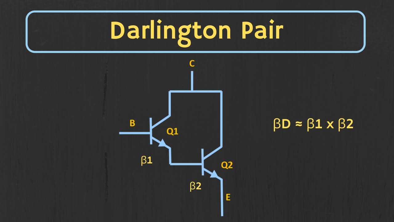
Darlington Pair Explained | The Darlington Pair as a Switch
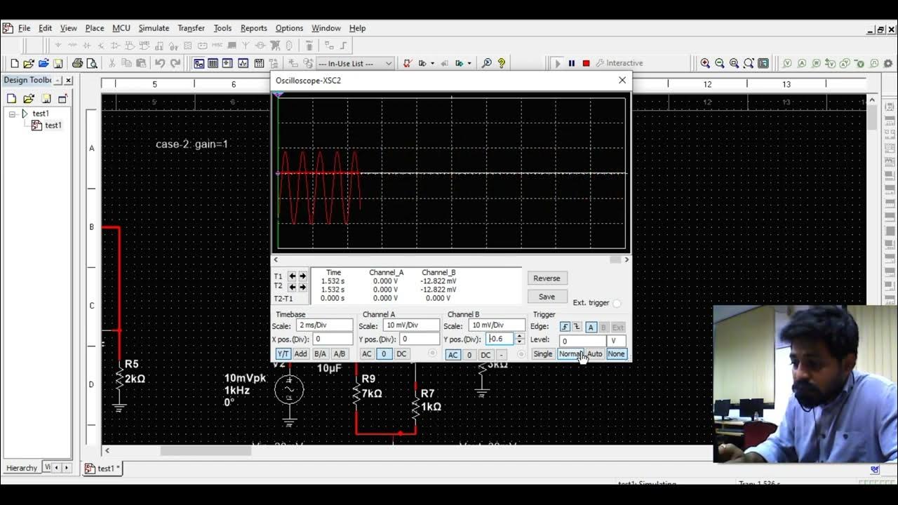
Multisim Tutorials --2: CE amplifier simulation part 1

Common-Emitter Configuration of a Transistor
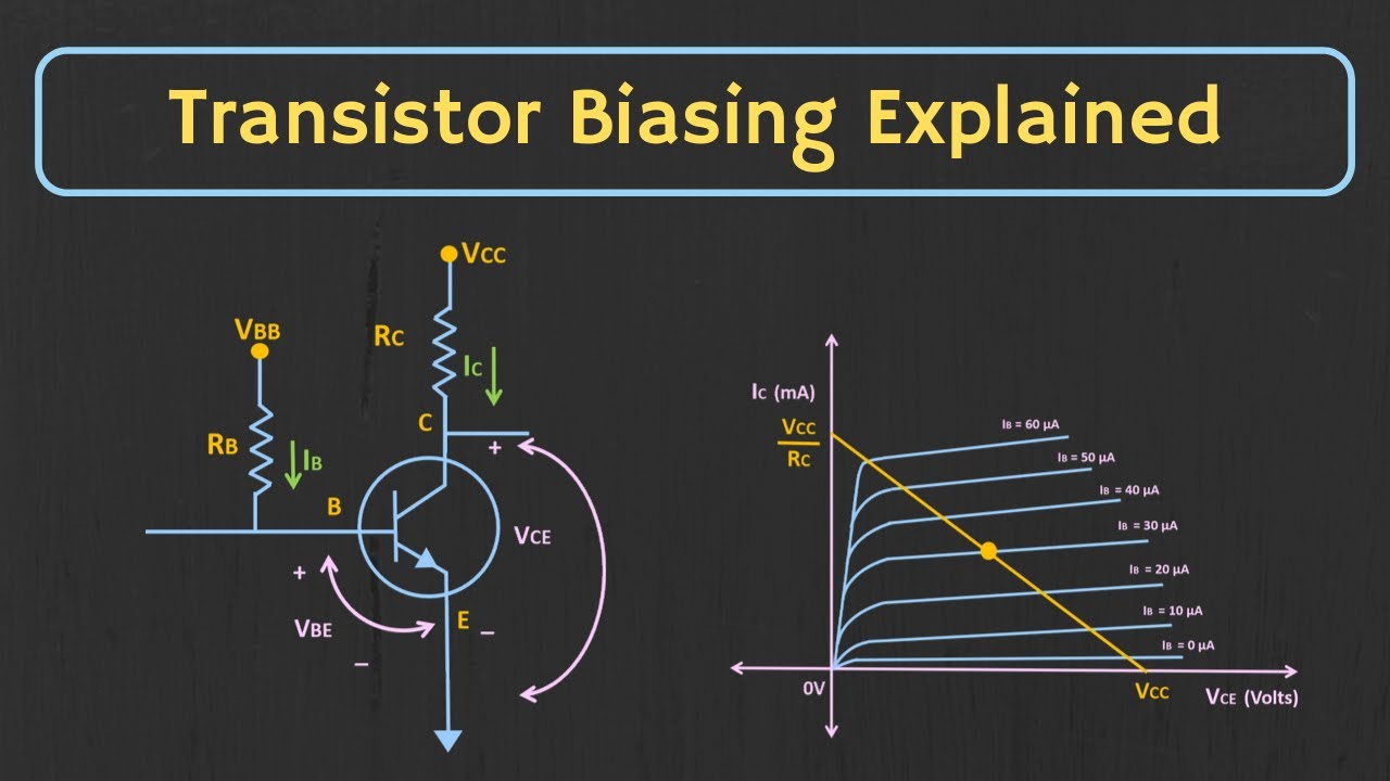
Transistor Biasing: What is Q-point? What is Load Line? Fixed Bias Configuration Explained
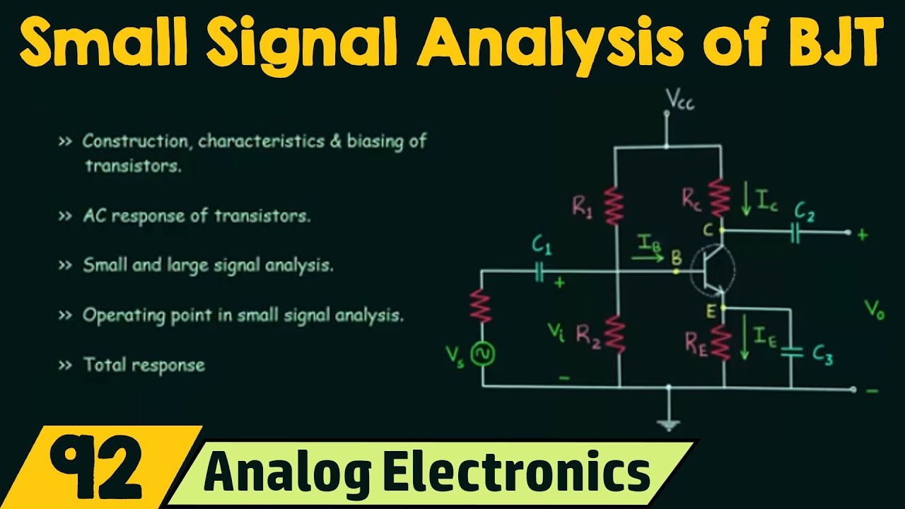
Small Signal Analysis of BJT
SUPERHETERODYNE Receiver - Modulation Techniques
5.0 / 5 (0 votes)